Avnet Xilinx Kintex-7 FPGA Mini-Module Plus开发方案
发布时间:2012-7-27 10:52
发布者:1770309616
|
Xilinx公司的Kintex-7 FPGA具有144GMACS DSP,能满足更高的性能而功耗是目前产品的40%,可以集成更多的硅器件,从而更容易创建差异性产品,具有更低的成本而提高了竞争性.可编程的Kintex-7 FPGA支持多种空中接口如LTE,WiMAX和WCDMA.广泛用在通信,医疗电子,3D TV,航空航天,多模式无线电等.本文介绍了Kintex-7 FPGA主要特性以及单片LTE基带(2x4MIMO)框图,手持超声波框图和IP网关视频框图与Kintex-7 Mini Module Plus开发套件主要特性,框图和板电源框图,开发套件电路图和材料清单. Kintex-7 FPGAs let designers build in superior bandwidth and 12-bit digitally programmable analog while meeting cost and power requirements. Unprecedented 144GMACS digital signal processor (DSP) power makes the versatile Kintex-7 devices an excellent option for applications such as portable ultrasound equipment and next-generation communications. Kintex-7 FPGAs deliver peak serial bandwidth (full duplex) of 800Gbps and include CPRI/OBSAI IP cores (9.8Gbps) optimized for today’s distributed baseband architectures. The programmable Kintex-7 devices can also be easily reconfigured to support multiple air interfaces such as LTE, WiMAX, and WCDMA. For interfacing to host systems, the Kintex-7 FPGA family provides built-in support for eight-channels of PCI Express (Gen1/Gen2). The highly efficient and affordable devices also enable designers to address connectivity and throughput requirements while minimizing part counts. The 72-bit, 1,833Mbps Kintex-7 memory interface supports single-memory-buffer designs instead of the two- or four-buffer designs required with other devices. Similarly, a single Kintex-7 device can process video at rates that enable a single-chip implementation of a video over IP gateway that can support 12 3G channels over a 4-channel 10 Gigabit Ethernet bridge. Kintex-7 FPGA 系列特性表: 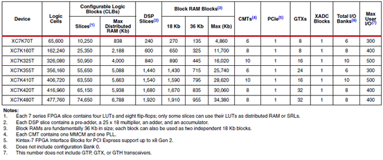
Kintex-7 FPGA主要特性: Twice the Price-Performance, Lower Cost • Many performance-boosting innovations including industry-leading 1,866Mbps memory interface; 639MHz DSP48E1 slices with high performance filtering capabilities; six-input look-up table • 1833Mbps memory interfaces • LVDS connectivity at 1.6G • Up to 1,920 DSP slices • Package optimized to line rate performance Memory Controller Innovations • Dedicated hard IP implementation of the memory Phy, for simplified interfacing to external DDR memory • A flexible, soft controller enabled by high-performance logic for calibration, access methods, and system interfaces • High-speed PCI Express hard and soft IP • Integrated hard IP for PCI Express, with full support for PCI Express endpoint and root port configurations • Hard IP support for up to eight PCI Express Gen1 and Gen2 channels • Soft IP support for up to eight PCI Express Gen3 channels Maximize Connectivity and Stay Within Budget • Kintex-7 FPGAs let designers choose a package with the right combination of price and performance for the application • Family price points each maximize throughput (6.6Gbps and 12.5Gbps transceivers) • Maximize performance with regular flip-chip BGA packaging offering highest signal integrity and up to 32 high-speed GTX transceivers (12.5Gbps line rates) • Minimize costs with bare-die flip-chip BGA packaging that delivers high signal integrity and robust thermal characteristics (up to 6.6Gbps line rates)Half the Power Consumption • HPL process cuts power in half compared to alternative 28nm High-Performance (HP) process • Low 1.0V core voltage (optional 0.9V core voltage option for some devices) translates into lower system power, lower cooling required, and more “green” designs •Additional power reductions from intelligent clock gating and fifth generation partial reconfiguration Kintex-7 FPGAs offer the best price-performance so designers can meet stringent latency requirements for LTE baseband processing in a common platform. • Programmability enables a cost-effective common platform supporting multiple air interfaces such as LTE, WiMAX, and WCDMA • Reduce total cost of ownership with the ability to scale and reuse designs from picocell to macrocell • 3x capacity at the same cost of previous-generation FPGAs while consuming 40% less power • Support for 9.8Gbps CPRI/OBSAI for high throughput • Support for 6.144Gbps CPRI/OBSAI in a low-cost package option 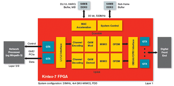
图1.单片LTE基带(2x4MIMO)框图 Support for 6.144Gbps CPRI/OBSAI in a low-cost package optionHigh I/O bandwidth and 144GMACS DSP processing power in chip-scale packaging make the Kintex-7 70T FPGA highly effective for both front- and back-end ultrasound processing. Designers can deploy a fully programmable 128-channel ultrasound implementation that scales up to 196 or 256 channels for high-end cart solutions or down to 64 or 32 channels for hand-held solutions. • 128-channel implementation in a modular set of five Kintex-7 70T FPGAs offers 44% lower power, 45% lower cost, and 57% smaller form factor compared to previous-generation FPGAs • Kintex-7 70T FPGAs offer 144GMACS from 240 DSP slices (288GMACS for symmetric filters) • Built-in support for eight PCI Express Gen1/Gen2 channels enables high-bandwidth interface to host system • Chip-scale packaging for small form factor 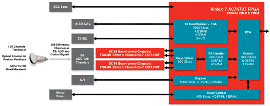
图2.手持超声波框图 Kintex-7 FPGAs enable cost-effective, low-power bridging of the serial digital interface (SDI) protocol onto IP technology for long-distance WAN transport to link local studios/live events, broadcast facilities, and satellite uplink stations using standard IP networks. • Reduce power by 64% and reduce cost by 85% with a single XC7K160T FPGA implementation of a 12x 3G-SDI over 4x10GbE bridge compared to the equivalent function implemented in two Virtex-6 XC6L130T devices • Reduce cost further with high-bandwidth interfaces that shrink BOM: 72-bit x 1,600Mbps DDR3 memory interface capability enables a single memory buffer that would require two or four memory buffers in previous-generation FPGAs. 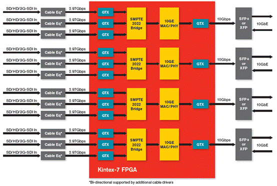
图3.IP网关视频框图 Kintex-7 Mini Module Plus开发套件 The Kintex-7 Mini Module Plus Development Kit provides a complete hardware environment for designers to accelerate their time to market. The kit delivers a stable platform to develop and test designs targeted to the high-performance and low-power Xilinx Kintex-7 325T FPGA. The installed Kintex-7 325T device offers a prototyping environment to effectively demonstrate the enhanced benefits of mid-range cost Xilinx FPGA solutions. Reference designs are included with the kit to exercise standard peripherals on the evaluation board for a quick start to device familiarization. Kintex-7 Mini Module Plus开发套件主要特性: Xilinx FPGA Devices Supported — Xilinx Kintex-7 XC7K160T-1FFG676 FPGA — Xilinx Kintex-7 XC7K325T-1FFG676 FPGA (Only option currently available) — Xilinx Kintex-7 XC7K410T-1FFG676 FPGA I/O Connectors — One Mini Module Plus Interface with JX1 / JX2 signal / power connectors, and JX3 power sense. — One 20 pin XADC Analog Header — One 10/100/1000 RJ-45 Ethernet Connector — One USB3 Micro B Connector — One USB3 JTAG fly-wire Header GTX Transceivers Accessed Through JX1/JX2 — One PCI Express interface 4 lanes @ 5.0 Gbps (PCI Express 2.0) — Four single lane General-Purpose MGT. Memory — 256MB of DDR3 memory (64M x 32) at 1600 Mbps — 64 MB of Flash memory in Master BPI configuration with a 50 MHz user CCLK. — 8KB of I2C EEPROM — 128KB of I2C EEPROM dedicated to EZ-USB FX3 SuperSpeed USB Controller Communication — EZ-USB FX3 SuperSpeed USB Controller — 10/100/1000 PHY Interface — RS232 Port accessed through JX1/JX2 — JTAG Port accessed through JX1/JX2 Clocks — 200MHz LVDS Clock Source — Programmable LVDS Clock Source (MGT reference clock input) — EMC LVCMOS 50MHz Clock Source — Dedicated 50MHz and 25MHz Clock Sources — Two MGT reference clock inputs available through JX1/JX2 — Four Differential clock inputs available through JX1/JX2 — Dedicated PHY receive and 125MHz clocks User I/O — 118 Differential IO available through JX1/JX2 Power — Regulated 3.3, 2.5, 1.8, 1.5, 1.2, 1.0 V supply voltages must be supplied through JX1/JX2 — Regulated 5.0, 1.8, 1.25 V analog supply voltages are generated on board Configuration — JTAG Port accessed through JX1/JX2 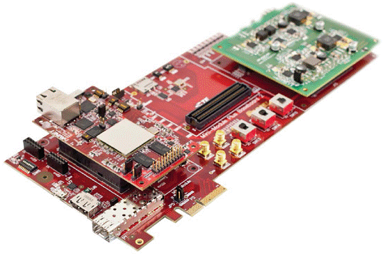
图4.装配好Kintex-7 Mini Module Plus开发套件外形图(不含电源或电缆) 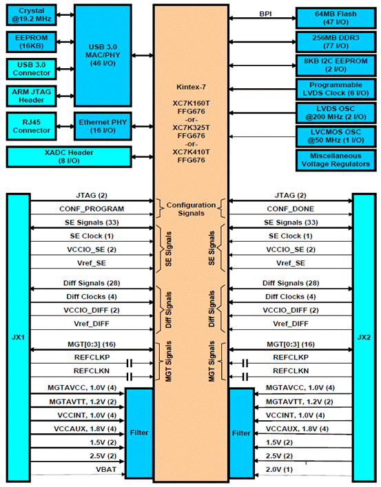
图5.Kintex-7 Mini Module Plus框图 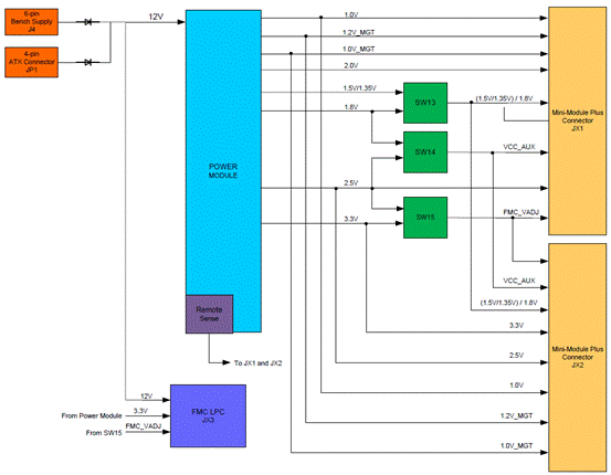
图6.Kintex-7 Mini Module Plus板电源框图 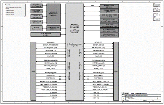
图7.Kintex-7 Mini Module Plus板电路图(1) 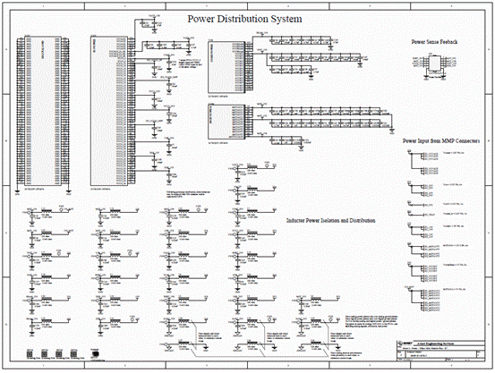
图8.Kintex-7 Mini Module Plus板电路图(2) 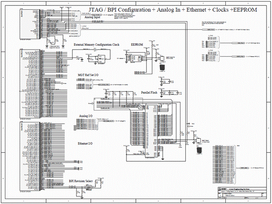
图9.Kintex-7 Mini Module Plus板电路图(3) 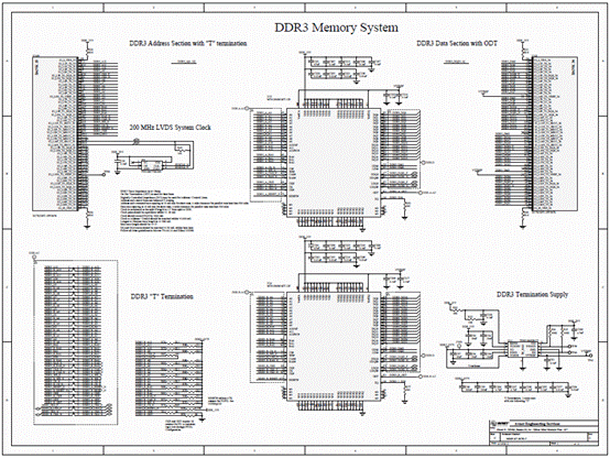
图10.Kintex-7 Mini Module Plus板电路图(4) 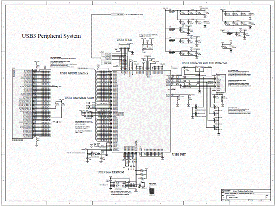
图11.Kintex-7 Mini Module Plus板电路图(5) 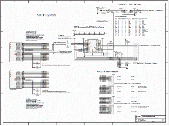
图12.Kintex-7 Mini Module Plus板电路图(6) 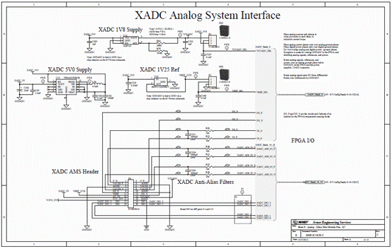
图13.Kintex-7 Mini Module Plus板电路图(7) 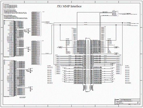
图14.Kintex-7 Mini Module Plus板电路图(8) 
图15.Kintex-7 Mini Module Plus板电路图(9) 
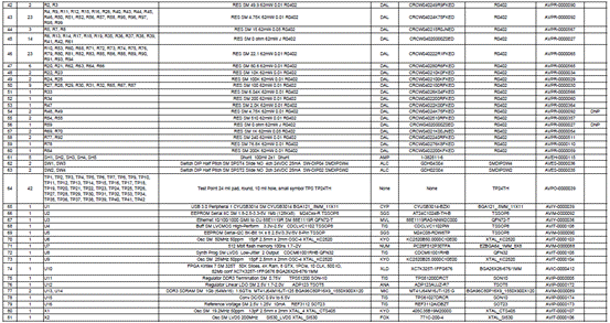
图16.Kintex-7 Mini Module Plus板电路图(10) Kintex-7 Mini Module Plus板材料清单: 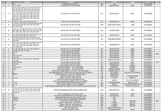
详情请见:  ds180_7Series_Overview.pdf
(579.11 KB)
和 https://www.em.avnet.com/Support%20And%20Downloads/AES-MMP-7K325T-G%20User%20Guide%20v1.0.pdf 以及 https://www.em.avnet.com/Support%20And%20Downloads/AES-MMP-7K325T-G_RevC_Schematic.PDF 来源:网络 |


网友评论