Keil MCBTWRK60 Tower系统Kinetis K60 MCU开发方案
发布时间:2012-8-31 11:21
发布者:1640190015
|
Keil 公司的MCBTWRK60 Tower系统能用来评估Freescale Kinetis K60系列器件MK60N512VMD100,为现在和未来产品开发确定硬件和软件.K60 MCU器件包括了IEEE 1588以太网,带充电器功能检测的全速和高速USB 2.0 OTG,硬件加密和篡改检测功能,闪存从256kB到1MB,并集成丰富的模拟,通信,时序和控制外设.本文介绍了Kinetis系列产品MCU主要特性和方框图,MCBTWRK60评估板技术指标和主要特性,评估板方框图以及K60N512 CPU板电路图,Primary Elevator板电路图,Secondary Elevator板电路图和串行接口板电路图. Kinetis is the most scalable portfolio of low power, mixed-signal ARM®Cortex™-M4 MCUs in the industry. Phase 1 of the portfolio consists of five MCU families with over 200 pin-,peripheral- and software-compatible devices. Each family offers excellent performance, memory and feature scalability with common peripherals, memory maps, and packages providing easy migration both within and between families. Kinetis MCUs are built from Freescale’s innovative 90nm Thin Film Storage (TFS) flash technology with unique FlexMemory (configurable embedded EEPROM). Kinetis MCU families combine the latest low-power innovations and high performance, high precision mixed-signal capability with a broad range of connectivity, human-machine interface, and safety & security peripherals. Kinetis MCUs are supported by a market-leading enablement bundle from Freescale and numerous ARM 3rd party ecosystem partners. Kinetis系列产品MCU主要特性表: 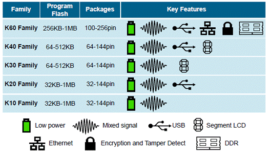
All Kinetis families include a powerful array of analog, communication and timing and control peripherals with the level of feature integration increasing with flash memory size and the number of inputs/outputs. Features common to all Kinetis families include: Kinetis系列产品MCU主要特性: • Core: ARM Cortex-M4 Core delivering 1.25DMIPS/MHz with DSP instructions (floating-point unit available on certain Kinetis families) • Up to 32-channel DMA for peripheral and memory servicing with minimal CPU intervention • Broad range of performance levels rated at maximum CPU frequencies of 50 MHz, 72 MHz, and 100 MHz (120 MHz, 150 MHz, and 180 MHz available on certain Kinetis families) • Ultra-low power: • 10 low power operating modes for optimizing peripheral activity and wake-up times for extended battery life. • Low–leakage wake-up unit, low power timer, and low power RTC for additional low power flexibility • Memory: Scalable memory footprints from 32 KB Flash / 8 KB RAM to 1 MB Flash / 128 KB RAM. Independent Flash banks enable concurrent code execution and firmware updates • Optional 16 KB cache memory for optimizing bus bandwidth and flash execution performance • FlexMemory with up to 512 KB FlexNVM and up to 16 KB FlexRAM. FlexMemory can be partitioned for data flash memory, EEPROM, or traditional RAM • Mixed-signal analog: Fast, high precision 16-bit ADCs, 12-bit DACs, programmable gain amplifiers, high speed comparators and an internal voltage reference. Powerful signal conditioning, conversion and analysis capability with reduced system cost • Human Machine Interface (HMI): • Capacitive Touch Sensing Interface with full low power support and minimal current adder when enabled • Connectivity and Communications: • UARTs with ISO7816 and IrDA support, I2S, CAN, I2C and DSPI • Reliability, Safety and Security:Hardware cyclic redundancy check engine for validating memory contents / communication data and increased system reliability • Independent-clocked COP for protection against code runaway in fail-safe applications • External watchdog monitor • Timing and Control: • Powerful FlexTimers which support general purpose, PWM, and motor control functions • Carrier Modulator Transmitter for IR waveform generation • Programmable Interrupt Timer for RTOS task scheduler time base or trigger source for ADC conversion and programmable delay block • External Interfaces: • Multi-function external bus interface capable of interfacing to external memories, gate-array logic, or an LCD • System: • 5 V tolerant GPIO with pin interrupt functionality • Wide operating voltage range from 1.71 V to 3.6 V with flash programmable down to 1.71 V with fully functional flash and analog peripherals • Ambient operating temperature ranges from -40 ℃ to 105 ℃ The K60 MCU family includes IEEE 1588 Ethernet, full- and high-speed USB 2.0 On-The-Go with device charger detect capability, hardware encryption and tamper detection capabilities. Devices start from 256 KB of flash in 100LQFP packages extending up to 1 MB in a 256MAPBGA package with a rich suite of analog, communication, timing and control peripherals. High memory density K60 family devices include an optional single precision floating point unit, NAND flash controller and DRAM controller. 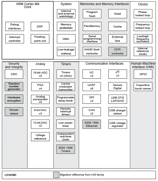
图1.K60方框图 The Keil MCBTWRK60 Tower System allows you to generate and test application programs for the Freescale Kinetis Kxx device family. With this hands-on process, you can determine the hardware and software requirements for current and future product development. This TWR-K60N512 board is populated with the Freescale Kinetis MK60N512VMD100 microcontroller. 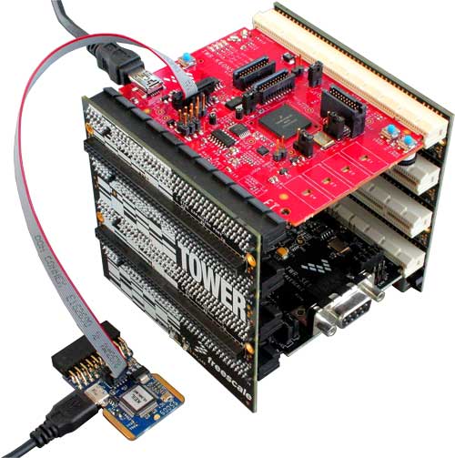
图2.MCBTWRK60入门套件外形图 MCBTWRK60评估板技术指标:
The MCBTWRK60 is designed to be a very flexible evaluation board for the Freescale Kinetis family of microprocessors. The MCBTWRK60 evaluation board can be expanded to build hardware prototypes. The Freescale Kinetis K60 microcontroller (U1) provided with the MCBTWRK60 board is a high-end MK60N512VMD100 device with advanced capabilities. A 50.0 MHz oscillator (Y1) provides the clock signal for the CPU when a jumper is installed on pins 1-2 of jumper J6. Moving the jumper to pins 2-3 allows external clocking from another board via the Primary Elevator. 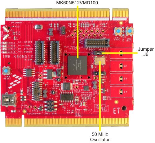
图3.MCBTWRK60评估板外形图 MCBTWRK60评估板主要特性: The connectors on the MCBTWRK60 evaluation board provide easy access to many of the on-chip peripherals. USB 2.0 Full Speed Interface Standard USB connectors for USB Device, USB-OTG, USB Host and UART via USB on the MCBTWRK60 board for applications requiring USB communications. Serial Port A standard DB9 connector on the Serial board for Kinetis’s serial port provides RS232 and RS485 connectivity. 100/10M Ethernet Port A standard RJ45 connector on the MCBTWRK60 Serial board connects to an on-board Ethernet transceiver for applications requiring Ethernet communications. CAN Interface A 3-pin header for applications requiring CAN communications on the MCBTWRK60 Serial board. Accelerometer A 3-axis accelerometer for detecting and measuring motion in 3 dimensions on the MCBTWRK60 Serial board. Touch Interface Four touch pads on the TWR-K60N512 board connected to the Touch Sensing Input module in the MCU allow them to be used as push buttons in your application.SD Card Connector A SD Card connector for developing applications requiring access to SD Cards.Analog Voltage Control for ADC Input An adjustable analog voltage source is on the TWR-K60N512 board for testing the Analog to Digital output feature of the Kinetis device. A configuration jumper enables and disables this feature. JTAG and Cortex/ETM Download and Debug The TWR-K60N512 board incorporates a Cortex Debug + ETM interface. When coupled with the ULINK2 USB-JTAG adapter, the Serial Wire JTAG interface allows flash programming and debugging. With the ULINKPro adapter, the Cortex Debug/ETM interface allows flash programming and instruction trace debugging. MCBTWRK60 Tower系统包括: The TWR-K60N512 Module. The TWR-SER Serial Module. The Primary and Secondary TWR-ELEV Elevator Modules. A µVision IDE Quick Start Guide. An ARM Development Tools Overview. The hardware block diagram displays input, configuration, power system, and User I/O on the TWR-K60 board and the Serial I/O board. This visual presentation helps you understand the MCBTWRK60 tower system components. 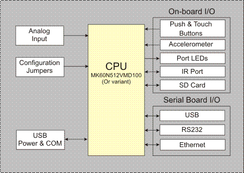
图4.MCBTWRK60评估板方框图 The Keil MCBTWRK60 comprises a number of boards, each has a separate schematic: 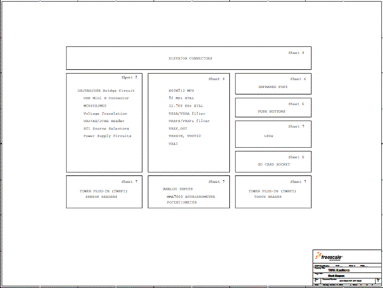
图5.K60N512 CPU板框图 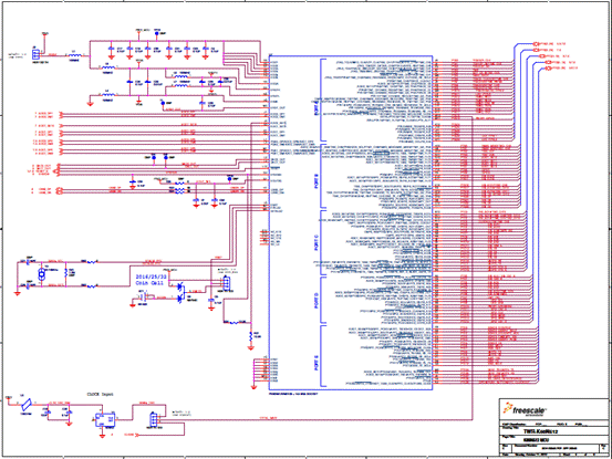
图6.K60N512 CPU板电路图(1) 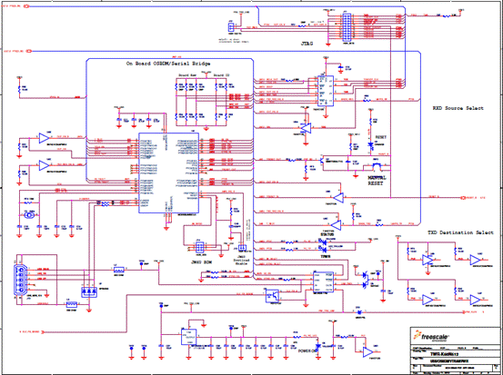
图7.K60N512 CPU板电路图(2) 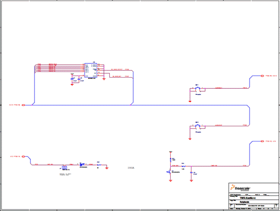
图8.K60N512 CPU板电路图(3) 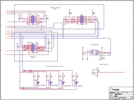
图9.K60N512 CPU板电路图(4) 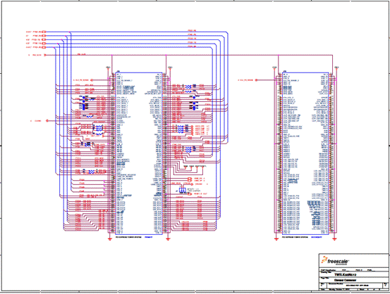
图10.K60N512 CPU板电路图(5) 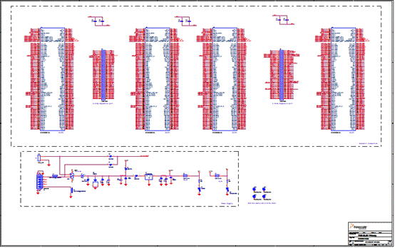
图11.Primary Elevator板电路图 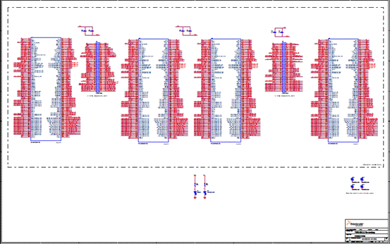
图12.Secondary Elevator板电路图 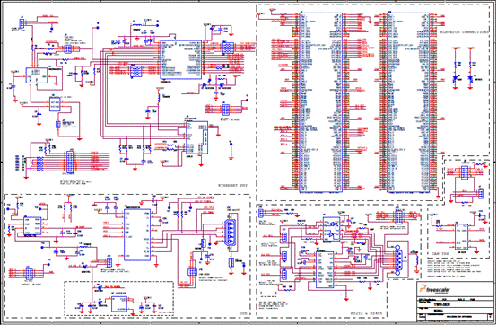
图13.串行接口板电路图 详情请见:  k60pb.pdf
(255.87 KB)
和  dui0553a_cortex_m4_dgug.pdf
(1.67 MB)
来源:网络 | |||||||||||||||||||||||||||||||||||||||||||||||||||||||||||||||||||



网友评论