ADI ADSP-BF609 Blackfin处理器高清视频开发方案
发布时间:2012-4-11 15:11
发布者:1770309616
|
ADI公司的ADSP-BF609是 Blackfin双核处理器,工作频率高达1GHz,硬件支持高清视频分析. ADSP-BF609采用ADI/INTEL微信号架构(MSA),每个核包含两个16位MAC,两个40位ALU和40位桶形移位RISC类寄存器和指令模式,具有先进的调试,跟踪和性能监视,主要用在从汽车电子到嵌入式工业,仪表和马达控制等应用.本文介绍了ADSP-BF609主要特性,方框图, Blackfin处理器核框图以及ADSP-BF609 EZ-KIT Lite®评估系统主要特性,框图,电路图和材料清单. The ADSP-BF609 processor is a member of the Blackfin family of products, incorporating the Analog Devices/Intel Micro Signal Architecture (MSA). Blackfin processors combine a dual-MAC state-of-the-art signal processing engine, the advantages of a clean, orthogonal RISC-like microprocessor instruction set, and single-instruction, multiple-data (SIMD) multimedia capabilities into a single instruction-set architecture. The processor offers performance up to 500 MHz, as well as low static power consumption. Produced with a low-power and lowvoltage design methodology, they provide world-class power management and performance. By integrating a rich set of industry-leading system peripherals and memory, Blackfin processors are the platform of choice for next-generation applications that require RISC-like programmability, multimedia support, and leadingedge signal processing in one integrated package. These applications span a wide array of markets, from automotive systems to embedded industrial, instrumentation and power/motor control applications. ADSP-BF609主要特性: Dual-core symmetric high-performance Blackfin processor, up to 500 MHz per core Each core contains two 16-bit MACs, two 40-bit ALUs, and a 40-bit barrel shifter RISC-like register and instruction model for ease of programming and compiler-friendly support Advanced debug, trace, and performance monitoring Pipelined Vision Processor provides hardware to process signal and image algorithms used for pre- and co-processing of video frames in ADAS or other video processing applications Accepts a range of supply voltages for I/O operation. Off-chip voltage regulator interface 349-ball (19 mm × 19 mm) RoHS compliant BGA package MEMORY Each core contains 148K bytes of L1 SRAM memory (processor core-accessible) with multi-parity bit protection Up to 256K bytes of L2 SRAM memory with ECC protection Dynamic memory controller provides 16-bit interface to a single bank of DDR2 or LPDDR DRAM devices Static memory controller with asynchronous memory interface that supports 8-bit and 16-bit memories Flexible booting options from flash, eMMC and SPI memories and from SPI, link port and UART hosts Memory management unit provides memory protection 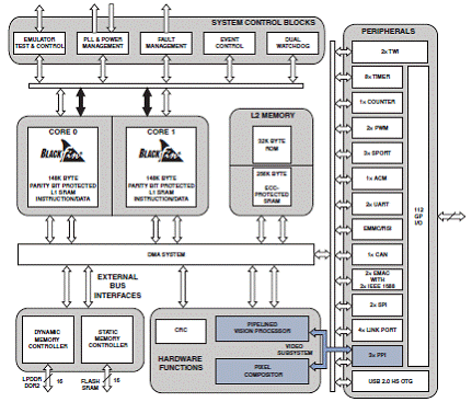
图1.ADSP-BF609处理器方框图 BLACKFIN处理器核 The processor integrates two Blackfin processor cores. Each core contains two 16-bit multipliers, two 40-bit accumulators, two 40-bit ALUs, four video ALUs, and a 40-bit shifter. The computation units process 8-, 16-, or 32-bit data from the register file. The compute register file contains eight 32-bit registers. When performing compute operations on 16-bit operand data, the register file operates as 16 independent 16-bit registers. All operands for compute operations come from the multiported register file and instruction constant fields. Each MAC can perform a 16-bit by 16-bit multiply in each cycle, accumulating the results into the 40-bit accumulators. Signed and unsigned formats, rounding, and saturation are supported. The ALUs perform a traditional set of arithmetic and logical operations on 16-bit or 32-bit data. In addition, many special instructions are included to accelerate various signal processing tasks. These include bit operations such as field extract and population count, modulo 232 multiply, divide primitives, saturation and rounding, and sign/exponent detection. The set of video instructions include byte alignment and packing operations,16-bit and 8-bit adds with clipping, 8-bit average operations, and 8-bit subtract/absolute value/accumulate (SAA) operations. Also provided are the compare/select and vector search instructions.For certain instructions, two 16-bit ALU operations can be performed simultaneously on register pairs (a 16-bit high half and 16-bit low half of a compute register). If the second ALU is used, quad 16-bit operations are possible. The 40-bit shifter can perform shifts and rotates and is used to support normalization, field extract, and field deposit instructions. The program sequencer controls the flow of instruction execution, including instruction alignment and decoding. For program flow control, the sequencer supports PC relative and indirect conditional jumps (with static branch prediction), and subroutine calls. Hardware supports zero-overhead looping. The architecture is fully interlocked, meaning that the programmer need not manage the pipeline when executing instructions with data dependencies. The address arithmetic unit provides two addresses for simultaneous dual fetches from memory. It contains a multiported register file consisting of four sets of 32-bit index, modify, length, and base registers (for circular buffering), and eight additional 32-bit pointer registers (for C-style indexed stack manipulation). Blackfin processors support a modified Harvard architecture in combination with a hierarchical memory structure. Level 1 (L1) memories are those that typically operate at the full processor speed with little or no latency. At the L1 level, the instruction memory holds instructions only. The data memory holds data, and a dedicated scratchpad data memory stores stack and local variable information. In addition, multiple L1 memory blocks are provided, offering a configurable mix of SRAM and cache. The memory management unit (MMU) provides memory protection for individual tasks that may be operating on the core and can protect system registers from unintended access. The architecture provides three modes of operation: user mode, supervisor mode, and emulation mode. User mode has restricted access to certain system resources, thus providing a protected software environment, while supervisor mode has unrestricted access to the system and core resources. 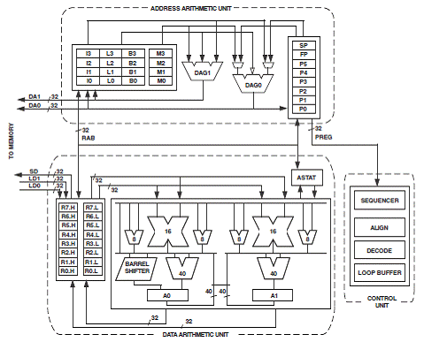
图2.Blackfin处理器核框图 ADSP-BF609 EZ-KIT Lite®评估系统 The ADSP-BF609 processor is a member of the Blackfin family of products,incorporating the Analog Devices/Intel Micro Signal Architecture (MSA). Blackfin processors combine a dual-MAC state-of-the-art signal processing engine, the advantages of a clean, orthogonal RISC-like microprocessor instruction set, and single-instruction, multiple-data (SIMD) multimedia capabilities into a single instruction-set architecture. ADSP-BF60x Blackfin processors embody a new type of embedded processor designed specifically to meet the computational demands and power constraints of today’s automotive systems, embedded industrial, instrumentation, and power/motor control applications. The evaluation board is designed to be used in conjunction with the CrossCore® Embedded Studio (CCES) development tools to test capabilities of the ADSP-BF60x Blackfin processors. The CCES development environment aids advanced application code development and debug, such as: • Create, compile, assemble, and link application programs written in C++,C, and assembly • Load, run, step, halt, and set breakpoints in application programs • Read and write data and program memory • Read and write core and peripheral registers • Plot memory Access to the processor from a personal computer (PC) is achieved through a USB port (when a debug agent is mounted on the EZ-KIT Lite board) or an external JTAG emulator. The USB interface provides unrestricted access to the ADSP-BF609 processor and evaluation board peripherals. Analog Devices JTAG emulators offer faster communication between the host PC and target hardware. Analog Devices carries a wide range of in-circuit emulation products. 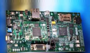
图3. ADSP-BF609 EZ-KIT Lite®评估板外形图 ADSP-BF609 EZ-KIT Lite®评估板主要特性: • Analog Devices ADSP-BF609 Blackfin processor • 349-pin LFBGA package • 25 MHz CLKIN oscillator • 48 MHz USB CLKIN • Double Data Rate Synchronous Dynamic Random-Access Memory (DDR2 SDRAM) • Micron MT47H64M16HR-3 • 64M x 16 bit (1 Gb) • Burst flash memory • Micron PC28F128P33T85B • 16M x 16-bit (32 MB) flash memory • Quad Serial Peripheral Interface (SPI) • Winbond W25Q32 • 32 Mb serial flash memory • Ethernet PHY • National Semiconductor • DP83848C 10/100 PHY • Two LEDs integrated into the RJ-45 connector: link/activity • Universal Asynchronous Receiver/Transmitter (UART) • ADM3315 RS-232 line driver/receiver • DB9 female connector • Temp sensor • On Semiconductor • ADM1032 two-wire sensor • Controller Area Network (CAN) • NXP TJA1041 • RJ-11 connector • Debug interface • JTAG header for use with ADI emulators • Standalone debug agent • LEDs • Eight LEDs: one power (green), one board reset (red), one temperature limit (amber), Ethernet speed (green), and four general-purpose (amber) • Push buttons • Four push buttons: one reset, one wake, and two IRQ/flag • Expansion Interface 3 (EI3) • Next generation of the expansion interface design, provides access to most of the processor signals • Power supply • CE approved • 5V @ 3.6 Amps • Other features • Link port connectors • SD/MMC memory connector • Rotary encoder • MP JTAG in and out connectors • 0.05-ohm resistors for processor current measurement • JTAG ICE 14-pin header • USB cable ADSP-BF609 EZ-KIT Lite®评估系统包括: • ADSP-BF609 EZ-KIT Lite board • Standalone debug agent (SADA2) • USB cable • 5 in 1 USB cable kit • CE approved power supply • Ethernet cable • 2 GB memory card • 4 nylon standoffs • 4 nylon hex nuts 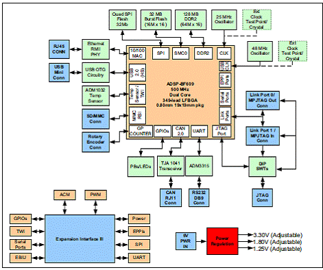
图4. ADSP-BF609 EZ-KIT Lite®评估板方框图 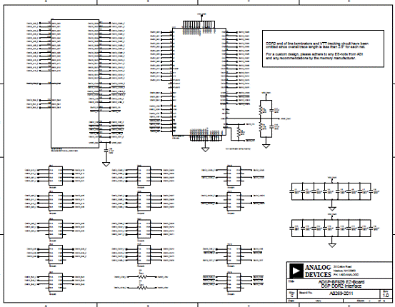
图5. ADSP-BF609 EZ-KIT Lite®评估板电路图(1) 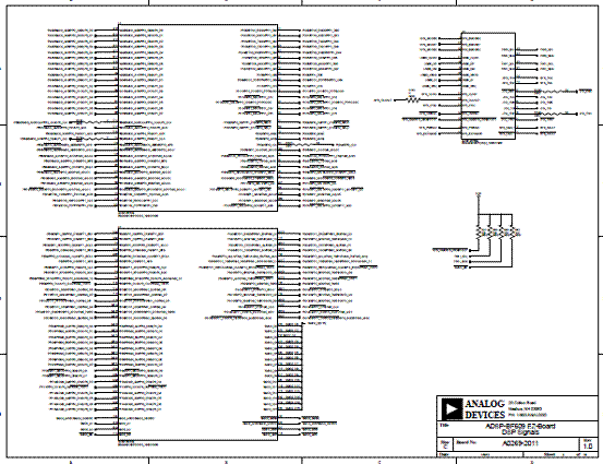
图6. ADSP-BF609 EZ-KIT Lite®评估板电路图(2) 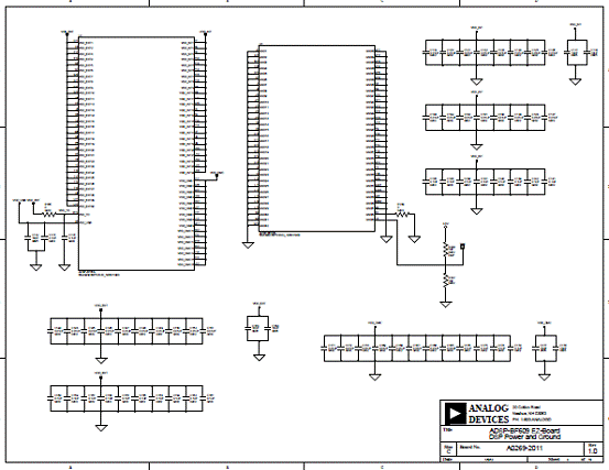
图7. ADSP-BF609 EZ-KIT Lite®评估板电路图(3) 
图8. ADSP-BF609 EZ-KIT Lite®评估板电路图(4) 
图9. ADSP-BF609 EZ-KIT Lite®评估板电路图(5) 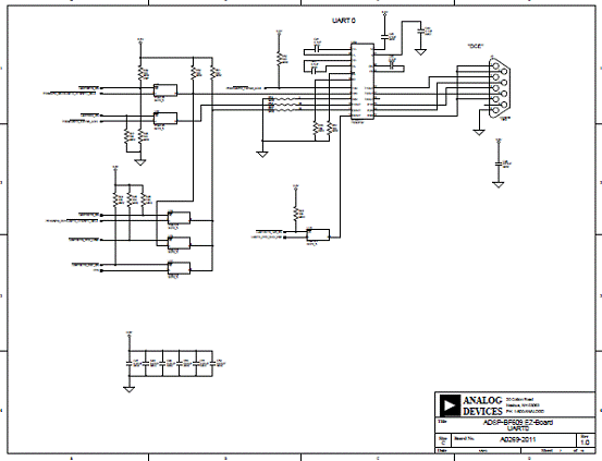
图10. ADSP-BF609 EZ-KIT Lite®评估板电路图(6) 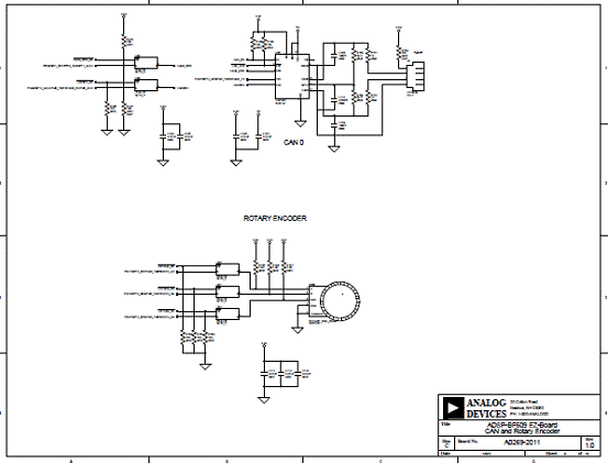
图11. ADSP-BF609 EZ-KIT Lite®评估板电路图(7) 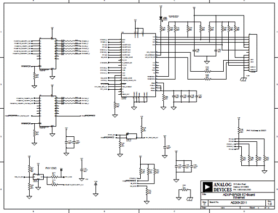
图12. ADSP-BF609 EZ-KIT Lite®评估板电路图(8) 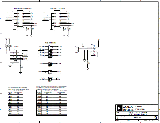
图13. ADSP-BF609 EZ-KIT Lite®评估板电路图(9) 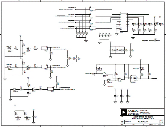
图14. ADSP-BF609 EZ-KIT Lite®评估板电路图(10) 
图15. ADSP-BF609 EZ-KIT Lite®评估板电路图(11) 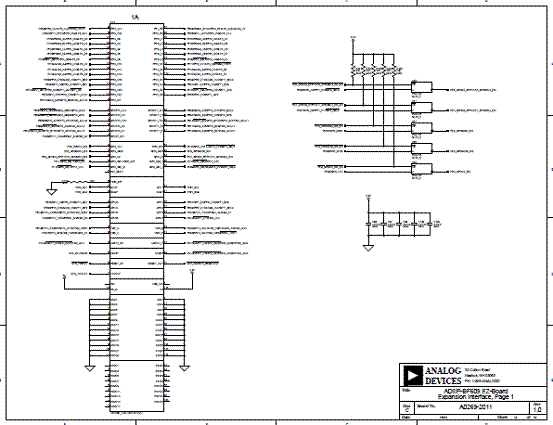
图16. ADSP-BF609 EZ-KIT Lite®评估板电路图(12) 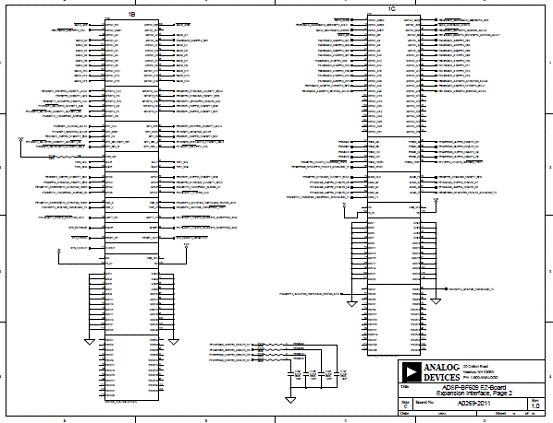
图17. ADSP-BF609 EZ-KIT Lite®评估板电路图(13) 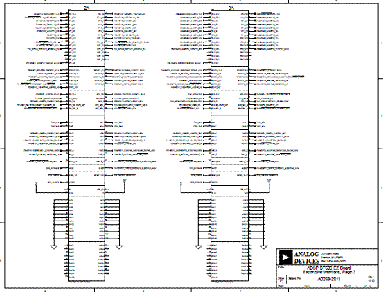
图18. ADSP-BF609 EZ-KIT Lite®评估板电路图(14) 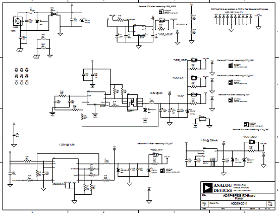
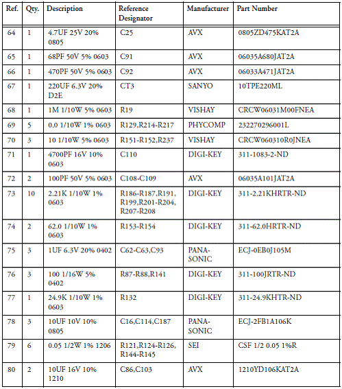
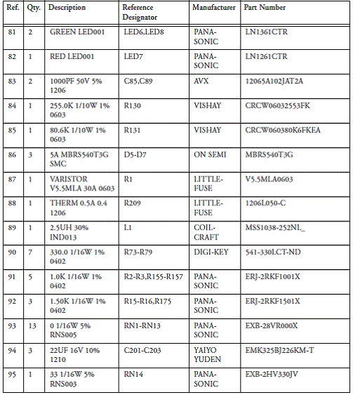
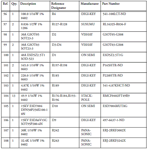
图19. ADSP-BF609 EZ-KIT Lite®评估板电路图(15) ADSP-BF609 EZ-KIT Lite®评估板材料清单(BOM): 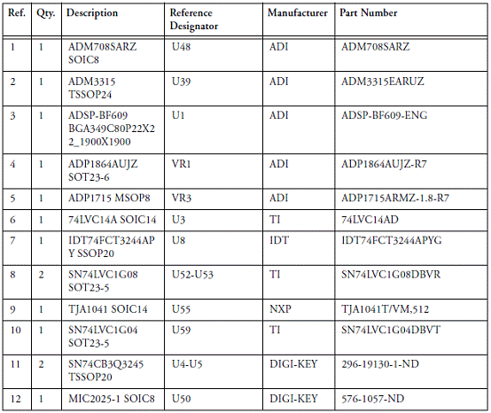
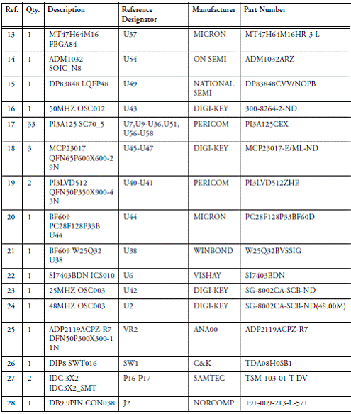
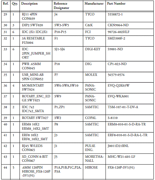
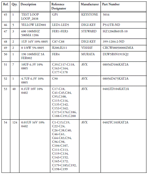

详情请见:  ADSP-BF606_607_608_609[2].pdf
(1.35 MB)
 ADSP-BF609_ezkit_man_rev_1-0_march_2012[2].pdf
(1.18 MB)
来源:网络 |


网友评论