Atmel AT32UC3A3256数字音频平台解决方案
发布时间:2011-11-28 21:59
发布者:1046235000
|
Atmel公司的AT32UC3A是采用AVR32 UC RISC处理器的系统级芯片(SoC)微控制器,工作频率高达66MHz,具有低功耗,高的代码密度和高性能,可实现存储器保护单元(MPU)和快速灵活的中断控制,支持现代操作系统和实时操作系统,采用DSP指令集可获得更高的计算功能,非常适合坞站,USB海量存储,SD卡播放,汽车立体声,USB扬声器,以及各种音/视频设备.本`文介绍了AT32UC3A主要特性, 方框图和UC3-A3 XPLAINED评估板主要特性与方框图. The AT32UC3A is a complete System-On-Chip microcontroller based on the AVR32 UC RISC processor running at frequencies up to 66 MHz. AVR32 UC is a high-performance 32-bit RISC microprocessor core, designed for cost-sensitive embedded applications, with particular emphasis on low power consumption, high code density and high performance. The processor implements a Memory Protection Unit (MPU) and a fast and flexible interrupt controller for supporting modern operating systems and real-time operating systems. Higher computation capabilities are achievable using a rich set of DSP instructions. The AT32UC3A incorporates on-chip Flash and SRAM memories for secure and fast access. For applications requiring additional memory, an external memory interface is provided on AT32UC3A0 derivatives. The Peripheral Direct Memory Access controller (PDCA) enables data transfers between peripherals and memories without processor involvement. PDCA drastically reduces processing overhead when transferring continuous and large data streams between modules within the MCU. The PowerManager improves design flexibility and security: the on-chip Brown-Out Detector monitors the power supply, the CPU runs from the on-chip RC oscillator or from one of external oscillator sources, a Real-Time Clock and its associated timer keeps track of the time. The Timer/Counter includes three identical 16-bit timer/counter channels. Each channel can be independently programmed to perform frequency measurement, event counting, interval measurement, pulse generation, delay timing and pulse width modulation. The PWM modules provides seven independent channels with many configuration options including polarity, edge alignment and waveform non overlap control. One PWM channel can trigger ADC conversions for more accurate close loop control implementations. The AT32UC3A also features many communication interfaces for communication intensive applications. In addition to standard serial interfaces like UART, SPI or TWI, other interfaces like flexible Synchronous Serial Controller, USB and Ethernet MAC are available. The Synchronous Serial Controller provides easy access to serial communication protocols and audio standards like I2S. The Full-Speed USB 2.0 Device interface supports several USB Classes at the same time thanks to the rich End-Point configuration. The On-The-GO (OTG) Host interface allows device like a USB Flash disk or a USB printer to be directly connected to the processor. The media-independent interface (MII) and reduced MII (RMII) 10/100 Ethernet MAC module provides on-chip solutions for network-connected devices. AT32UC3A integrates a class 2+ Nexus 2.0 On-Chip Debug (OCD) System, with non-intrusive real-time trace, full-speed read/write memory access in addition to basic runtime control. AT32UC3A主要特性: • High Performance, Low Power AVR®32 UC 32-Bit Microcontroller – Compact Single-cycle RISC Instruction Set Including DSP Instruction Set – Read-Modify-Write Instructions and Atomic Bit Manipulation – Performing 1.49 DMIPS / MHz Up to 91 DMIPS Running at 66 MHz from Flash (1 Wait-State) Up to 49 DMIPS Running at 33MHz from Flash (0 Wait-State) – Memory Protection Unit • Multi-hierarchy Bus System – High-Performance Data Transfers on Separate Buses for Increased Performance – 15 Peripheral DMA Channels Improves Speed for Peripheral Communication • Internal High-Speed Flash – 512K Bytes, 256K Bytes, 128K Bytes Versions – Single Cycle Access up to 33 MHz – Prefetch Buffer Optimizing Instruction Execution at Maximum Speed – 4ms Page Programming Time and 8ms Full-Chip Erase Time – 100,000 Write Cycles, 15-year Data Retention Capability – Flash Security Locks and User Defined Configuration Area • Internal High-Speed SRAM, Single-Cycle Access at Full Speed – 64K Bytes (512KB and 256KB Flash), 32K Bytes (128KB Flash) • External Memory Interface on AT32UC3A0 Derivatives – SDRAM / SRAM Compatible Memory Bus (16-bit Data and 24-bit Address Buses) • Interrupt Controller – Autovectored Low Latency Interrupt Service with Programmable Priority • System Functions – Power and Clock Manager Including Internal RC Clock and One 32KHz Oscillator – Two Multipurpose Oscillators and Two Phase-Lock-Loop (PLL) allowing Independant CPU Frequency from USB Frequency – Watchdog Timer, Real-Time Clock Timer • Universal Serial Bus (USB) – Device 2.0 Full Speed and On-The-Go (OTG) Low Speed and Full Speed – Flexible End-Point Configuration and Management with Dedicated DMA Channels – On-chip Transceivers Including Pull-Ups • Ethernet MAC 10/100 Mbps interface – 802.3 Ethernet Media Access Controller – Supports Media Independent Interface (MII) and Reduced MII (RMII) • One Three-Channel 16-bit Timer/Counter (TC) – Three External Clock Inputs, PWM, Capture and Various Counting Capabilities • One 7-Channel 16-bit Pulse Width Modulation Controller (PWM) • Four Universal Synchronous/Asynchronous Receiver/Transmitters (USART) – Independant Baudrate Generator, Support for SPI, IrDA and ISO7816 interfaces – Support for Hardware Handshaking, RS485 Interfaces and Modem Line • Two Master/Slave Serial Peripheral Interfaces (SPI) with Chip Select Signals • One Synchronous Serial Protocol Controller – Supports I2S and Generic Frame-Based Protocols • One Master/Slave Two-Wire Interface (TWI), 400kbit/s I2C-compatible • One 8-channel 10-bit Analog-To-Digital Converter • 16-bit Stereo Audio Bitstream –Sample Rate Up to 50 KHz • On-Chip Debug System (JTAG interface) – Nexus Class 2+, Runtime Control, Non-Intrusive Data and Program Trace • 100-pin TQFP (69 GPIO pins), 144-pin LQFP (109 GPIO pins) , 144 BGA (109 GPIO pins) • 5V Input Tolerant I/Os • Single 3.3V Power Supply or Dual 1.8V-3.3V Power Supply 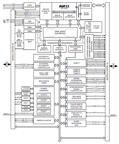
图1. AT32UC3A方框图 UC3-A3 XPLAINED评估板 The Atmel UC3-A3 XPLAINED evaluation kit is a hardware platform to evaluate the Atmel AT32UC3A3256 microcontroller. The kit offers a large range of features that enables the Atmel AVR® UC3 user to get started using UC3 peripherals right away and understand how to integrate the UC3 device in their own design. UC3-A3 XPLAINED评估板主要特性: • Atmel® AT32UC3A3256 microcontroller • 64Mbit SDRAM • Analog input (to ADC) - Temperature sensor - RC filter • I/O - One mechanical button - Four LEDs - Four expansion headers • Footprints for external memory - Atmel AT45DB series DataFlash® serial flash - Atmel AT25DF series industry standard serial flash • Touch - One Atmel QTouch® slider - One Atmel QTouch button 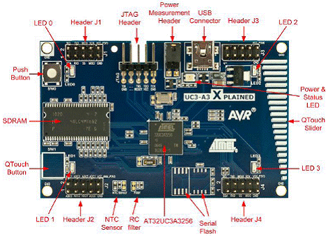
图2.UC3-A3 XPLAINED评估板外形图 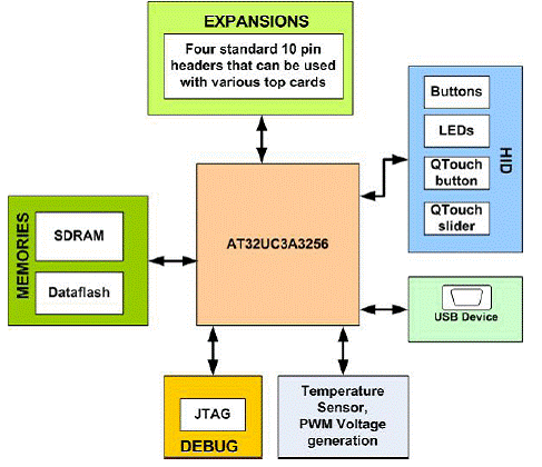
图3.UC3-A3 XPLAINED评估板框图 详情请见:  32058S[1].pdf
(1.4 MB)
 doc32159[1].pdf
(365.68 KB)
|


网友评论