Microchip dsPIC33E数字信号控制器USB入门开发方案
发布时间:2011-7-12 13:52
发布者:Liming
|
Microchip公司的dsPIC33E和PIC24E系列是高性能的16位数字信号控制器和位控制器,3.0V-3.6V时的性能高达60MIPS,MCU的CPU采用改进的哈佛架构,16位宽数据通路和24位宽指令,DSC的CPU具有11条附加指令,两个40位累加器,可进行16x16分数乘/除运算,双数据提取,单周期乘法和累加。支持高端的工业控制和通信应用,包括伺服马达控制,太阳能逆变器以及运行两个并联三相马达等。本文介绍了dsPIC33E和PIC24E系列主要特性,方框图和dsPIC33E USB入门套件主要特性,框图和电路图,PCB布局图。 dsPIC33E和PIC24E系列主要特性: Operating Range: • Up to 60 MIPS Operation (at 3.0V-3.6V): - Industrial temperature range (-40℃ to +85℃) - Extended temperature range (-40℃ to +125℃) High-Performance MCU CPU: (All Devices) • Modified Harvard Architecture • C Compiler Optimized Instruction Set • 16-bit Wide Data Path • 24-bit Wide Instructions • Linear Program Memory Addressing up to 4M Instruction Words • Linear Data Memory Addressing up to 64 Kbytes • 73 Base Instructions: mostly with an effective instruction execution throughput of one instruction per cycle • Flexible and Powerful Indirect Addressing mode • Software Stack • 16x16 Integer Multiply Operations • 32/16 and 16/16 Integer Divide Operations • Up to ±16-bit Shifts Additional High-Performance DSC CPU Features dsPIC33EPXXXMU806/810/814 Devices Only) • 11 Additional Instructions • Two 40-bit Accumulators with Rounding and Saturation Options • Additional Flexible and Powerful Addressing modes: - Modulo - Bit-Reversed • Single-Cycle Multiply and Accumulate: - Accumulator write back for DSP operations - Dual data fetch • Single-Cycle shifts for up to 40-bit Data • 16x16 Fractional Multiply/Divide Operations Direct Memory Access (DMA): • 15-Channel Hardware DMA: - Allows for transfer of data to/from any data memory location • Up to 4 Kbytes Dual Ported DMA Buffer Area (DPSRAM) to store data transferred via DMA: - Allows for fast data transfer between RAM and a peripheral while CPU is executing code (no cycle stealing) • Most Peripherals Support DMA Interrupt Controller: • 13-Cycle Fixed Latency or 9- to 13-Cycle Variable Latency (user-selectable) • Up to 116 Available Interrupt Sources • Up to Five External Interrupts • Seven Programmable Priority Levels • Seven Processor Exceptions Timers/Capture/Compare/PWM: • Timer/Counters, up to Nine 16-bit Timers: - Can pair up to make four 32-bit timers - One timer runs as a Real-Time Clock with an external 32.768 kHz oscillator - Programmable prescaler • Input Capture (up to 16 channels): - Independent 16-bit time base - Capture on up, down or both edges - 16-bit capture input functions - 4-deep FIFO on each capture - Synchronous, Triggered and Cascaded modes • Output Compare (up to 16 channels): - Independent 16-bit time base - Single or Dual 16-bit Compare mode - 16-bit Glitchless PWM mode - Synchronous, Triggered and Cascaded modes • Hardware Real-Time Clock and Calendar (RTCC): Provides clock, calendar, and alarm functions Digital I/O: • Peripheral Pin Select (PPS) Functionality • Wake-up/Interrupt-on-Change for up to 122 pins • Output Pins can drive from 3.0V to 3.6V • Up to 5V Output with Open Drain Configuration • Up to 8 or 10 mA sink on I/O pins • Up to 8 mA or 12 mA source on I/O pins On-Chip Flash and SRAM: • Flash Program Memory (up to 512 Kbytes) • Flash Auxiliary Memory (up to 24 Kbytes): - Can be used as Bootloader space or for EEPROM emulation without stalling the CPU • Data SRAM (up to 52 Kbytes) • Read/Write Security for Program Flash and Auxiliary Memory System Management: • Flexible Clock Options: - External, crystal, resonator, internal RC - Fully integrated Phase-Locked Loop (PLL) - Extremely low jitter PLL - Auxiliary PLL for USB clocking - Reference clock output • Programmable Power-up Timer • Oscillator Start-up Timer • Watchdog Timer with its own RC Oscillator • Fail-Safe Clock Monitor • Multiple Reset Sources Power Management: • On-chip 1.8V Voltage Regulator • Switch between Clock Sources in Real Time • Idle, Sleep, and Doze modes with Fast Wake-up CMOS Flash Technology: • Low-Power, High-Speed Flash Technology • Fully Static Design • 3.3V (±10%) Operating Voltage • Industrial and Extended Temperature • Low-Power Consumption Analog-to-Digital Converters (ADCs): • 10-bit, 1.1 Msps or 12-bit, 500 Ksps Conversion: - Two and four simultaneous samples (10-bit mode) - Up to 32 input channels with auto-scanning - Conversion start can be manual or synchronized with one of 13 trigger sources - Conversions in Sleep mode - ±2 LSb max integral nonlinearity - ±1 LSb max differential nonlinearity • Additional 10-bit, 1.1 Msps ADC, with up to 16 Input Channels Data Converter Interface (DCI) Module: (dsPIC33EPXXXMU806/810/814 Devices Only) • Codec Interface • Supports I2S and AC’97 Protocols • Up to 16-bit Data Words, up to 16 Words per Frame: 4-word deep TX and RX buffers Comparator Module: • Three Analog Comparators with Programmable Input/Output Configuration • Blanking and Filtering Options • Internal or External Voltage References Motor Control Peripherals: (dsPIC33EPXXXMU806/810/814 Devices Only) • Motor Control PWM: - Two master time base modules can control dual 3-phase motors simultaneously - Up to seven PWM generators - Two PWM outputs per PWM generator - Individual period and duty cycle for each PWM output - Dead-time insertion and correction - Duty cycle, dead time, phase shift and frequency resolution of 8.32 ns - Seven independent Fault and current-limit inputs - Center-Aligned, Edge-Aligned, Push-Pull, Multi-Phase, Variable Phase, Fixed Off-time, Current Reset and Current Limit modes - Output override control - Output Chopping (gated) mode - Special Event Triggers Motor Control Peripherals (Continued): (dsPIC33EPXXXMU806/810/814 Devices Only) • Quadrature Encoder Interface (QEI): - 32-bit position counter - 32-bit Index pulse counter - 32-bit Interval timer - 16-bit velocity counter - 32-bit Position Initialization/Capture/Compare High register - 32-bit Position Compare Low register - x4 Quadrature Count mode - External Up/Down Count mode - External Gated Count mode - External Gated Timer mode - Internal Timer mode Communication Modules: • USB On-The-Go (OTG): - USB v2.0 On-The-Go (OTG) compliant - Dual role capable – can act as either Host or Peripheral - Low-speed (1.5 Mbps) and Full-speed (12 Mbps) USB operation in Host mode - High-precision PLL for USB - Supports up to 32 endpoints (16 bidirectional): • USB module can use any RAM location on the device as USB endpoint buffers: - On-chip USB transceiver - Interface for Off-chip USB transceiver - On-chip pull-up and pull-down resistors • 4-wire SPI (up to four modules): - Framing supports I/O interface to simple codecs - Supports 8-bit and 16-bit data - Supports all serial clock formats and sampling modes • I2C™ (up to two modules): - Full Multi-Master Slave mode support - 7-bit and 10-bit addressing - Bus collision detection and arbitration - Integrated signal conditioning - Slave address masking - IPMI support - SMBus support Communication Modules (Continued): • UART (up to four modules): - Interrupt on address bit detect - Interrupt on UART error - Wake-up on Start bit from Sleep mode - 4-character TX and RX FIFO buffers - LIN bus support - IrDA® encoding and decoding in hardware - High-Speed Baud mode - Hardware Flow Control with CTS and RTS • Enhanced CAN (ECAN™) 2.0B active (up to two modules): - Up to eight transmit and up to 32 receive buffers - 16 receive filters and three masks - Loopback, Listen Only and Listen All - Messages modes for diagnostics and bus monitoring - Wake-up on CAN message - Automatic processing of Remote Transmission Requests - FIFO mode using DMA - DeviceNet™ addressing support • Parallel Master Slave Port (PMP/EPSP): - Supports 8-bit or 16-bit data - Supports up to 16 address lines • Programmable Cyclic Redundancy Check (CRC): - Programmable bit length for the CRC generator polynomial (up to 32-bit length) - 4x32, 8x16 or 16x8 FIFO for data input Packaging: • 64-pin QFN (9x9x0.9 mm) • 64-pin TQFP (10x10x1 mm) • 100-pin TQFP (12x12x1 mm) • 100-pin TQFP (14x14x1 mm) • 121-pin BGA (10x10x1.2 mm) • 144-pin LQFP (20x20x1.4 mm) • 144-pin TQFP (16x16x1 mm) 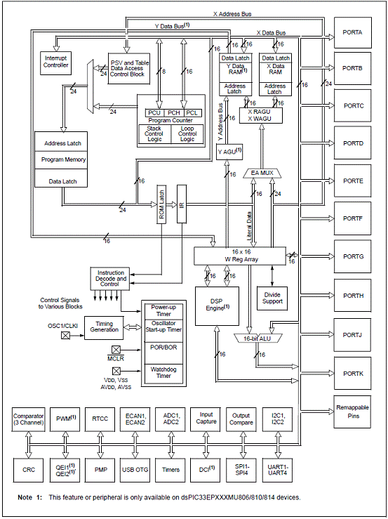
图1。dsPIC33EPXXXMU806/810/814和PIC24EPXXXGU810/814方框图 dsPIC33E USB入门套件 The starter kit comes preloaded with demonstration software for the user to explore the new features of the dsPIC33E DSC family (dsPIC33E USB Starter Kit) or the PIC24E MCU family (PIC24E USB Starter Kit). It is also expandable through a modular expansion interface, which allows the user to extend its functionality. The starter kit also supplies on-board circuitry for full debug and programming capabilities. dsPIC33E USB入门套件包括: The starter kit contains the following items: • dsPIC33E or PIC24E USB Starter Kit Development Board • dsPIC33E or PIC24E USB Starter Kit Information Sheet • USB mini-B to full-sized A cable - USB debug cable to debug and power the board • USB micro-B to full-sized A cable - USB cable to communicate with the dsPIC33E/PIC24E USB device port 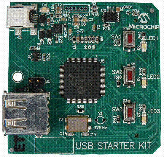
图2。dsPIC33E USB入门套件外形图 dsPIC33E USB入门套件主要特性: The top assembly of the board includes these key features: 1. dsPIC33EP512MU810 16-bit DSC device (dsPIC33E USB Starter Kit) or PIC24EP512GU810 16-bit MCU (PIC24E USB Starter Kit). 2. Green power indicator LED (D4). 3. 8 MHz crystal (Y3) for precision microcontroller clocking. 4. USB connectivity for on-board debugger communications (J2). 5. Three push button switches (SW1, SW2, SW3) for user-defined inputs. 6. Three user-defined indicator LEDs (LED1, LED2, LED3). 7. USB Type A receptacle (J6) connectivity for dsPIC33E/PIC24E USB host-based applications. 8. HOST mode power jumper (J5). 9. Regulated +3.3V power supply for powering the starter kit via USB or an expansion board. 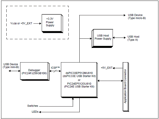
图3。dsPIC33E USB入门套件框图 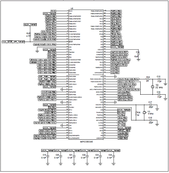
图4。dsPIC33E USB入门版电路图(目标器件:dsPIC33E/PIC24E) 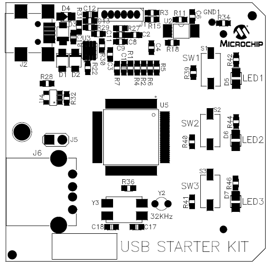
图5。dsPIC33E USB入门版电路图:电源分布/开关 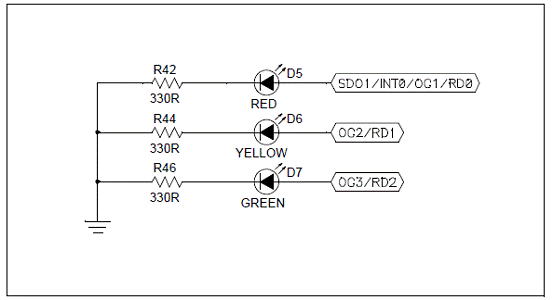
图6。dsPIC33E USB入门版电路图:用户LED 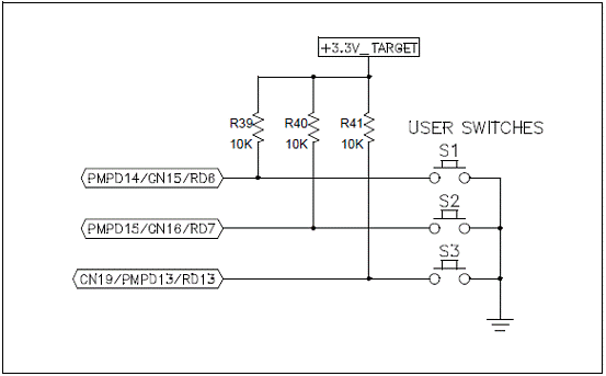
图7。dsPIC33E USB入门版电路图:用户开关 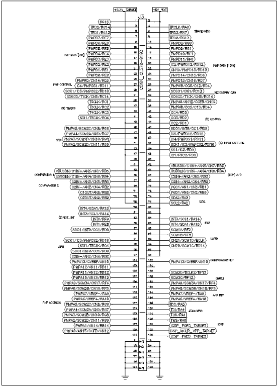
图8。dsPIC33E USB入门版电路图:接口 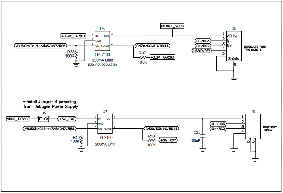
图9。dsPIC33E USB入门版电路图:USB连接 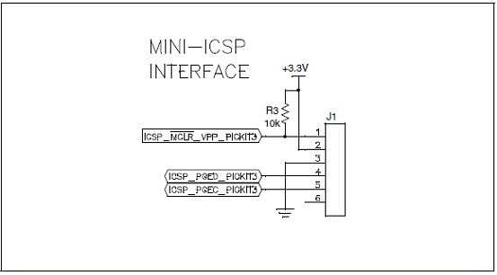
图10。dsPIC33E USB入门版电路图:MINI-ICSP接口 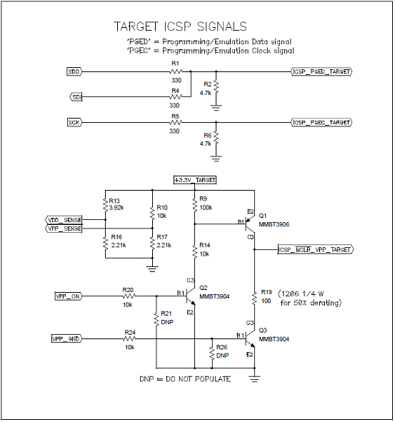
图11。dsPIC33E USB入门版电路图:串行EEPROM 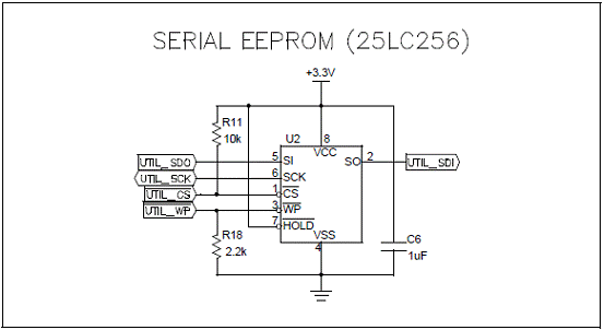
图12。dsPIC33E USB入门版电路图:目标ICSP信号 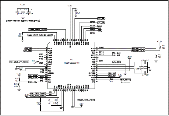
图13。dsPIC33E USB入门版电路图:D PIC24FJ256GB106主调试器 
图14。dsPIC33E USB入门版布局图(顶层) 详情请见: http://ww1.microchip.com/downloads/en/DeviceDoc/DS70616C.pdf 和 http://ww1.microchip.com/downloads/en/DeviceDoc/33E_24E_USB_SK_UserGuide.pdf |




网友评论