TI ADS1299多路低噪音EEG模拟前端解决方案
发布时间:2012-9-15 20:29
发布者:1770309616
|
TI公司的ADS1299是8路低噪音同时取样的24位delta-sigma ADC,并内置了可编程增益放大器(PGA),基准电压和振荡器,集成了脑电图(EEG)所需的通用特性.器件具有非常低的输入参考噪音:1.0 μVPP (70-Hz BW),没路的功耗5mW,输入偏置电流300pA,数据速率250SPS到16kSPS,C1.0 μVPP (70-Hz BW),CMMR为-110dB,可编程增益为1, 2, 4, 6, 8, 12或24,单极或双极电源工作,主要用在医疗仪器如EEG和ECG,听觉诱发电位(EAP),脑电双频谱指数(BIS),睡眠研究监测等,高精度多路信号采集.本文介绍了ADS1299主要特性,功能框图,单电源和双极电源工作电路,以及评估板ADS1299EEG-FE主要特性,框图,电路图,材料清单和PCB布局图. The ADS1299 is a low-noise, multichannel, simultaneous-sampling, 24-bit, delta-sigma (ΔΣ) analog-to-digital converter (ADC) with a built-in programmable gain amplifier (PGA), internal reference, and an onboard oscillator. The ADS1299 incorporates all commonly-required features for electroencephalogram (EEG) applications. With its high levels of integration and exceptional performance, the ADS1299 enables the creation of 23scalable medical instrumentation systems at significantly reduced size, power, and overall cost. The ADS1299 has a flexible input multiplexer per channel that can be independently connected to the internally-generated signals for test, temperature, and lead-off detection. Additionally, any configuration of input channels can be selected for derivation of the patient bias output signal. The ADS1299 operates at data rates from 250 SPS to 16 kSPS. Lead-off detection can be implemented internal to the device, either with an external pull-up or pull-down resistor or an excitation current sink or source. Multiple ADS1299 devices can be cascaded in high channel count systems in a daisy-chain configuration. The ADS1299 is offered in a TQFP-64 package specified from –40℃ to +85℃. ADS1299主要特性: • Eight Low-Noise PGAs and Eight High- Resolution Simultaneous-Sampling ADCs • Very Low Input-Referred Noise: 1.0 μVPP (70-Hz BW) • Low Power: 5 mW/channel • Input Bias Current: 300 pA • Data Rate: 250 SPS to 16 kSPS • CMRR: –110 dB • Programmable Gain: 1, 2, 4, 6, 8, 12, or 24 • Unipolar or Bipolar Supplies: – Analog: 4.75 V to 5.25 V – Digital: 1.8 V to 3.6 V . • Built-In Bias Drive Amplifier, Lead-Off Detection, Test Signals • Built-In Oscillator • Internal or External Reference • Flexible Power-Down, Standby Mode • Pin-Compatible with the ADS1298IPAG • SPI™-Compatible Serial Interface • Operating Temperature Range: –40℃ to +85℃ ADS1299应用: • Medical Instrumentation (EEG and ECG) Including: – EEG, Bispectral index (BIS), Evoked audio potential (EAP), Sleep study monitor • High-Precision, Simultaneous, Multichannel Signal Acquisition 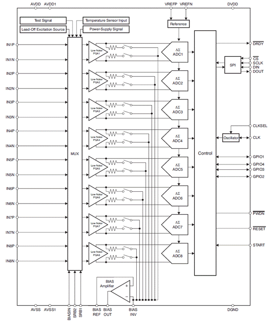
图1.ADS1299功能框图 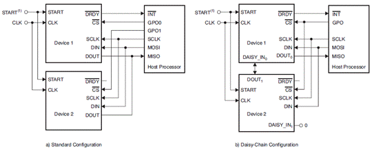
图2.多个ADS1299器件配置图 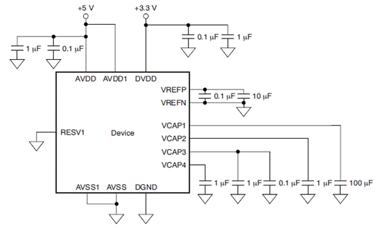
图3.ADS1299单电源工作电路图 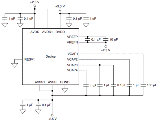
图4.ADS1299双极电源工作电路图 脑电图(EEG)前端性能演示板ADS1299EEG-FE This user’s guide describes the characteristics, operation, and use of the ADS1299EEG-FE. This EVM is an evaluation module for the ADS1299, an eight-channel, 24-bit, low-power; integrated analog front-end (AFE) designed for electroencephalography (EEG) applications. The ADS1299ECG-FE is intended for prototyping and evaluation. This user’s guide includes a complete circuit description, schematic diagram, and bill of materials. The ADS1299EEG-FE is intended for evaluating the ADS1299 low-power, low noise 24-bit, simultaneously sampling, eight-channel front-end for EEG applications. The digital SPI™ control interface is provided by the MMB0 Modular EVM motherboard (Rev. D or higher) that connects to the ADS1299EEG FE evaluation board (Rev A). The ADS1299EEG-FE is NOT a reference design for EEG applications; rather, its purpose is to expedite evaluation and system development. The output of the ADS1299 yields a raw, unfiltered EEG signal. The MMB0 motherboard allows the ADS1299EEG-FE to be connected to the computer via an available USB port. This manual shows how to use the MMB0 as part of the ADS1299EEG-FE, but does not provide technical details about the MMB0 itself. Throughout this document, the abbreviation EVM and the term evaluation module are synonymous with the ADS1299EEG-FE. ADS1299EEG-FE支持的特性: Hardware Features: • Configurable for bipolar or unipolar supply operation • Configurable for internal and external clock and reference via jumper settings • Configurable for dc-coupled inputs • External bias electrode drive • Option to provide a common reference to all channels negative terminals. • Option to select any electrode as reference electrode • Option to choose any electrode as bias electrode • External shield drive amplifier Software Features: • Analysis tools including a virtual oscilloscope, histogram, FFT. • Data export for post-processing of raw EEG data 
图5.ADS1299EEG-FE外形图 ADS1299EEG-FE 包括: • ADS1299EEG FE printed circuit board (PCB), Rev A • MMB0 (Modular EVM motherboard, Rev D or higher) • Universal ac to dc wall adapter, 120V to 240V ac to +6V dc 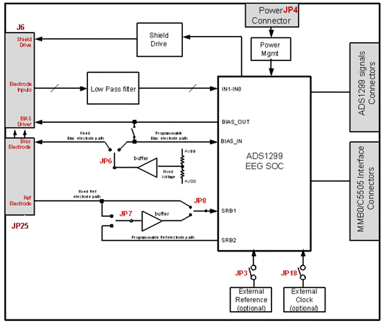
图6.ADS1299 EEG-FE前端框图 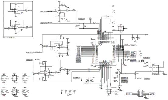
图7.ADS1299EEG-FC电路图 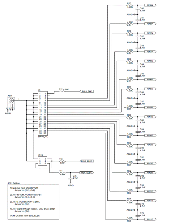
图8.ADS1299EEG-FC跨接器电路图 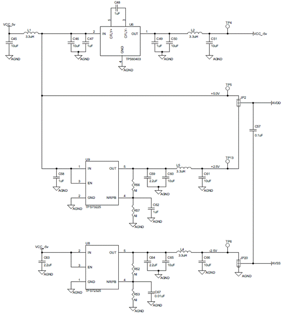
图9.ECG电源 
图10.外接基准驱动器(未安装) 
图11.ECG MDK板接口适配器电路 ADS1299 EEG-FE材料清单(BOM): 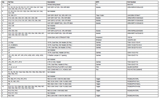

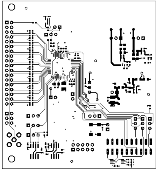
图12.ADS1299EEG-FE PCB布局图(顶层) 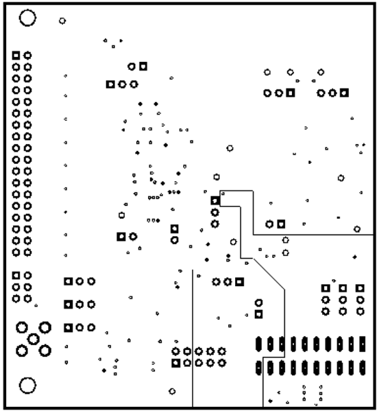
图13.ADS1299EEG-FE PCB布局图(中间层1) 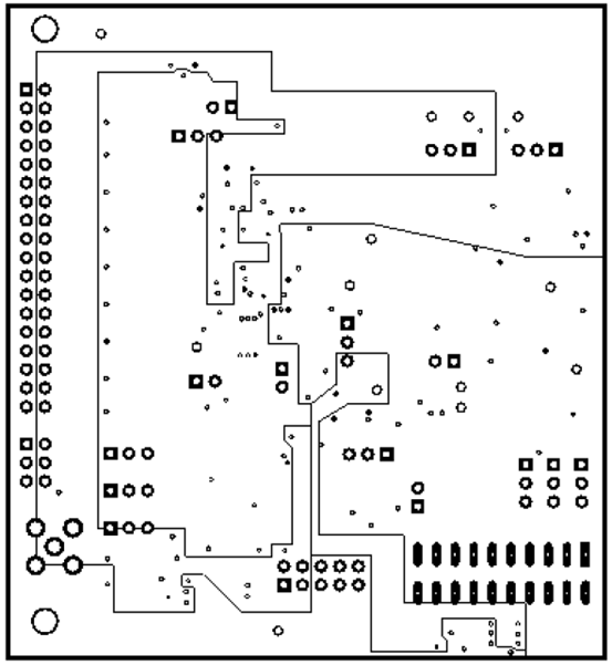
图14.ADS1299EEG-FE PCB布局图(中间层2) 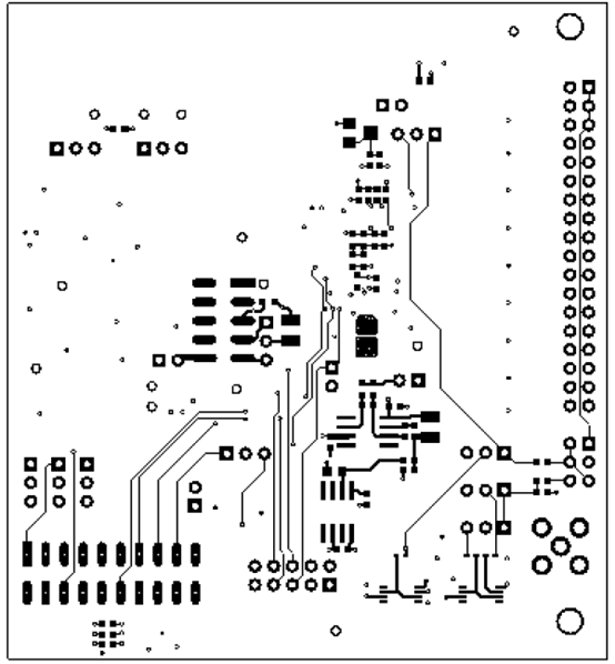
图15.ADS1299EEG-FE PCB布局图(底层) 
图16.ADS1299EEG-FE底层元件布局图 详情请见:  sbas499a.pdf
(1.64 MB)
和  slau443.pdf
(3.17 MB)
来源:网络 |






网友评论