Freescale MPC5634M 32位MCU开发方案
发布时间:2012-7-24 13:01
发布者:1770309616
|
Freescale 公司的MPC5634M是基于Power Architecture®的32位MCU,用户模式100%和Power Architecture 指令集兼容,工作频率0 MHz-80 MHz ,工作温度到+150度C,具有低功耗性能,工作电压4.5 V-5.25 V,内部稳压器提供3.3V和1.2V用于内核和逻辑电路,主要用于气油引擎管理,摩托车引擎控制,混合动力汽车,热量表和温度控制器,CAN等.本文介绍了MPC5634M主要特性,框图,TRK-MPC5634M低成本开发系统主要特性,电路图和PCB元件布局图. This document provides electrical specifications, pin assignments, and package diagrams for the MPC5634M series of microcontroller units (MCUs). For functional characteristics, refer to the MPC5634M Microcontroller Reference Manual. The MPC5634M series microcontrollers are system-on-chip devices that are built on Power Architecture® technology and: • Are 100% user-mode compatible with the Power Architecture instruction set • Contain enhancements that improve the architecture’s fit in embedded applications • Include additional instruction support for digital signal processing (DSP) • Integrate technologies such as an enhanced time processor unit, enhanced queued analog-to-digital converter, Controller Area Network, and an enhanced modular input-output system MPC5634M主要特性: • Operating Parameters — Fully static operation, 0 MHz – 80 MHz (plus 2% frequency modulation - 82 MHz) — –40 degreeC to 150 degreeC junction temperature operating range — Low power design – Less than 400 mW power dissipation (nominal) – Designed for dynamic power management of core and peripherals – Software controlled clock gating of peripherals – Low power stop mode, with all clocks stopped — Fabricated in 90 nm process — 1.2 V internal logic — Single power supply with 5.0 V -10%/+5% (4.5 V to 5.25 V) with internal regulator to provide 3.3 V and 1.2 V for the core — Input and output pins with 5.0 V -10%/+5% (4.5 V to 5.25 V) range – 35%/65% VDDE CMOS switch levels (with hysteresis) – Selectable hysteresis – Selectable slew rate control — Nexus pins powered by 3.3 V supply — Designed with EMI reduction techniques – Phase-locked loop – Frequency modulation of system clock frequency – On-chip bypass capacitance – Selectable slew rate and drive strength • High performance e200z335 core processor — 32-bit Power Architecture Book E programmer’s model — Variable Length Encoding Enhancements – Allows Power Architecture instruction set to be optionally encoded in a mixed 16 and 32-bit instructions – Results in smaller code size — Single issue, 32-bit Power Architecture technology compliant CPU — In-order execution and retirement — Precise exception handling — Branch processing unit – Dedicated branch address calculation adder – Branch acceleration using Branch Lookahead Instruction Buffer — Load/store unit – One-cycle load latency – Fully pipelined – Big and Little Endian support – Misaligned access support – Zero load-to-use pipeline bubbles — Thirty-two 64-bit general purpose registers (GPRs) — Memory management unit (MMU) with 16-entry fully-associative translation look-aside buffer (TLB) — Separate instruction bus and load/store bus — Vectored interrupt support — Interrupt latency < 120 ns @ 80 MHz (measured from interrupt request to execution of first instruction of interrupt exception handler) — Non-maskable interrupt (NMI) input for handling external events that must produce an immediate response, e.g., power down detection. On this device, the NMI input is connected to the Critical Interrupt Input. (May not be recoverable) — Critical Interrupt input. For external interrupt sources that are higher priority than provided by the Interrupt Controller. (Always recoverable) — New ‘Wait for Interrupt’ instruction, to be used with new low power modes — Reservation instructions for implementing read-modify-write accesses — Signal processing extension (SPE) APU – Operating on all 32 GPRs that are all extended to 64 bits wide – Provides a full compliment of vector and scalar integer and floating point arithmetic operations (including integer vector MAC and MUL operations) (SIMD) – Provides rich array of extended 64-bit loads and stores to/from extended GPRs – Fully code compatible with e200z6 core — Floating point (FPU) – IEEE 754 compatible with software wrapper – Scalar single precision in hardware, double precision with software library – Conversion instructions between single precision floating point and fixed point – Fully code compatible with e200z6 core — Long cycle time instructions, except for guarded loads, do not increase interrupt latency — Extensive system development support through Nexus debug port • Advanced microcontroller bus architecture (AMBA) crossbar switch (XBAR) — Three master ports, four slave ports – Masters: CPU Instruction bus; CPU Load/store bus (Nexus); eDMA – Slave: Flash; SRAM; Peripheral Bridge; calibration EBI — 32-bit internal address bus, 64-bit internal data bus • Enhanced direct memory access (eDMA) controller — 32 channels support independent 8-bit, 16-bit, or 32-bit single value or block transfers — Supports variable sized queues and circular queues — Source and destination address registers are independently configured to post-increment or remain constant — Each transfer is initiated by a peripheral, CPU, or eDMA channel request — Each eDMA channel can optionally send an interrupt request to the CPU on completion of a single value or block transfer • Interrupt controller (INTC) — 191 peripheral interrupt request sources — 8 software setable interrupt request sources — 9-bit vector – Unique vector for each interrupt request source – Provided by hardware connection to processor or read from register — Each interrupt source can be programmed to one of 16 priorities — Preemption – Preemptive prioritized interrupt requests to processor – ISR at a higher priority preempts ISRs or tasks at lower priorities – Automatic pushing or popping of preempted priority to or from a LIFO – Ability to modify the ISR or task priority. Modifying the priority can be used to implement the Priority Ceiling Protocol for accessing shared resources. — Low latency—three clocks from receipt of interrupt request from peripheral to interrupt request to processor • Frequency Modulating Phase-locked loop (FMPLL) — Reference clock pre-divider (PREDIV) for finer frequency synthesis resolution — Reduced frequency divider (RFD) for reducing the FMPLL output clock frequency without forcing the FMPLL to re-lock — System clock divider (SYSDIV) for reducing the system clock frequency in normal or bypass mode — Input clock frequency range from 4 MHz to 20 MHz before the pre-divider, and from 4 MHz to 16 MHz at the FMPLL input — Voltage controlled oscillator (VCO) range from 256 MHz to 512 MHz — VCO free-running frequency range from 25 MHz to 125 MHz — Four bypass modes: crystal or external reference with PLL on or off — Two normal modes: crystal or external reference — Programmable frequency modulation – Triangle wave modulation – Register programmable modulation frequency and depth — Lock detect circuitry reports when the FMPLL has achieved frequency lock and continuously monitors lock status to report loss of lock conditions – User-selectable ability to generate an interrupt request upon loss of lock – User-selectable ability to generate a system reset upon loss of lock — Clock quality monitor (CQM) module provides loss-of-clock detection for the FMPLL reference and output clocks – User-selectable ability to generate an interrupt request upon loss of clock – User-selectable ability to generate a system reset upon loss of clock – Backup clock (reference clock or FMPLL free-running) can be applied to the system in case of loss of clock • Calibration bus interface (EBI) — Available only in the calibration package (496 CSP package) — 1.8 V to 3.3 V ± 10% I/O (1.6 V to 3.6 V) — Memory controller with support for various memory types — 16-bit data bus, up to 22-bit address bus — Selectable drive strength — Configurable bus speed modes — Bus monitor — Configurable wait states • System integration unit (SIU) — Centralized GPIO control of 80 I/O pins — Centralized pad control on a per-pin basis – Pin function selection – Configurable weak pull-up or pull-down – Drive strength – Slew rate – Hysteresis — System reset monitoring and generation — External interrupt inputs, filtering and control — Critical Interrupt control — Non-Maskable Interrupt control — Internal multiplexer subblock (IMUX) – Allows flexible selection of eQADC trigger inputs (eTPU, eMIOS and external signals) – Allows selection of interrupt requests between external pins and DSPI • Error correction status module (ECSM) — Configurable error-correcting codes (ECC) reporting — Single-bit error correction reporting • On-chip flash memory — Up to 1.5 MB flash memory, accessed via a 64-bit wide bus interface — 16 KB shadow block — Fetch Accelerator – Provide single cycle flash access at 80 MHz – Quadruple 128-bit wide prefetch/burst buffers – Prefetch buffers can be configured to prefetch code or data or both — Censorship protection scheme to prevent flash content visibility — Flash divided into two independent arrays, allowing reading from one array while erasing/programming the other array (used for EEPROM emulation) — Memory block: – For MPC5634M: 18 blocks (4 x16 KB, 2 x32 KB, 2 x64 KB, 10 x128 KB) – For MPC5633M: 14 blocks (4 x16 KB, 2 x32 KB, 2 x64 KB, 6 x128 KB) – For MPC5632M: 12 blocks (4 x16 KB, 2 x32 KB, 2 x64 KB, 4 x128 KB) — Hardware programming state machine • On-chip static RAM — For MPC5634M: 94 KB general purpose RAM of which 32 KB are on standby power supply — For MPC5633M: 64 KB general purpose RAM of which 32 KB are on standby power supply — For MPC5632M: 48 KB general purpose RAM of which 24 KB are on standby power supply • Boot assist module (BAM) — Enables and manages the transition of MCU from reset to user code execution in the following configurations: – Execution from internal flash memory – Execution from external memory on the calibration bus – Download and execution of code via FlexCAN or eSCI • Periodic interrupt timer (PIT) — 32-bit wide down counter with automatic reload — Four channels clocked by system clock — One channel clocked by crystal clock — Each channel can produce periodic software interrupt — Each channel can produce periodic triggers for eQADC queue triggering — One channel out of the five can be used as wake-up timer to wake device from low power stop mode • System timer module (STM) — 32-bit up counter with 8-bit prescaler — Clocked from system clock — Four-channel timer compare hardware — Each channel can generate a unique interrupt request — Designed to address AUTOSAR task monitor function • Software watchdog timer (SWT) — 32-bit timer — Clock by system clock or crystal clock — Can generate either system reset or non-maskable interrupt followed by system reset — Enabled out of reset • Enhanced modular I/O system (eMIOS) — 16 timer channels (up to 14 channels in 144 LQFP) — 24-bit timer resolution — Supports a subset of the timer modes found in eMIOS on MPC5554 — 3 selectable time bases plus shared time or angle counter bus from eTPU2 — DMA and interrupt request support — Motor control capability • Second-generation enhanced time processor unit (eTPU2) — Object-code compatible with eTPU—no changes are required to hardware or software if only eTPU features are used — Intelligent co-processor designed for timing control — High level tools, assembler and compiler available — 32 channels (each channel has dedicated I/O pin in all packages) — 24-bit timer resolution — 14 KB code memory and 3 KB data memory — Double match and capture on all channels — Angle clock hardware support — Shared time or angle counter bus with eMIOS — DMA and interrupt request support — Nexus Class 1 debug support — eTPU2 enhancements – Counters and channels can run at full system clock speed – Software watchdog – Real-time performance monitor – Instruction set enhancements for smaller more flexible code generation – Programmable channel mode for customization of channel operation • Enhanced queued A/D converter (eQADC) — Two independent on-chip redundant signed digit (RSD) cyclic ADCs – 8-, 10-, and 12-bit resolution – Differential conversions – Targets up to 10-bit accuracy at 500 KSample/s (ADC_CLK = 7.5 MHz) and 8-bit accuracy at 1 MSample/s (ADC_CLK = 15 MHz) for differential conversions – Differential channels include variable gain amplifier (VGA) for improved dynamic range (x1; x2; x4) – Differential channels include programmable pull-up and pull-down resistors for biasing and sensor diagnostics(200 kohm; 100 k0hm; low value of 5 k0hm) – Single-ended signal range from 0 to 5 V – Sample times of 2 (default), 8, 64 or 128 ADC clock cycles – Provides time stamp information when requested – Parallel interface to eQADC command FIFOs (CFIFOs) and result FIFOs (RFIFOs) – Supports both right-justified unsigned and signed formats for conversion results – Temperature sensor to enable measurement of die temperature – Ability to measure all power supply pins directly — Automatic application of ADC calibration constants – Provision of reference voltages (25% VREF and 75% VREF) for ADC calibration purposes — Up to 341 input channels available to the two on-chip ADCs — Four pairs of differential analog input channels — Full duplex synchronous serial interface to an external device – Has a free-running clock for use by the external device – Supports a 26-bit message length – Transmits a null message when there are no triggered CFIFOs with commands bound for external CBuffers, or when there are triggered CFIFOs with commands bound for external CBuffers but the external CBuffers are full — Parallel Side Interface to communicate with an on-chip companion module — Zero jitter triggering for queue 0. (Queue 0 trigger causes current conversion to be aborted and the queued conversions in the CBUFFER to be bypassed. Delay from Trigger to start of conversion is 13 system clocks + 1 ADC clock.) — eQADC Result Streaming. Generation of a continuous stream of ADC conversion results from a single eQADC command word. Controlled by two different trigger signals; one to define the rate at which results are generated and the other to define the beginning and ending of the stream. Used to digitize waveforms during specific time/angle windows, e.g., engine knock sensor sampling. — Angular Decimation. The ability of the eQADC to sample an analog waveform in the time domain, perform Finite Impulse Response (FIR) or Infinite Impulse Response (IIR) filtering also in the time domain, but to down sample the results in the angle domain. Resulting in a time domain filtered result at a given engine angle. — Priority Based CFIFOs – Supports six CFIFOs with fixed priority. The lower the CFIFO number, the higher its priority. When commands of distinct CFIFOs are bound for the same CBuffer, the higher priority CFIFO is always served first. – Supports software and several hardware trigger modes to arm a particular CFIFO – Generates interrupt when command coherency is not achieved — External Hardware Triggers – Supports rising edge, falling edge, high level and low level triggers – Supports configurable digital filter — Supports four external 8-to-1 muxes which can expand the input channel number from 341 to 59 • Two deserial serial peripheral interface modules (DSPI) — SPI – Full duplex communication ports with interrupt and DMA request support – Supports all functional modes from QSPI subblock of QSMCM (MPC5xx family) – Support for queues in RAM – 6 chip selects, expandable to 64 with external demultiplexers – Programmable frame size, baud rate, clock delay and clock phase on a per frame basis – Modified SPI mode for interfacing to peripherals with longer setup time requirements – LVDS option for output clock and data to allow higher speed communication — Deserial serial interface (DSI) – Pin reduction by hardware serialization and deserialization of eTPU, eMIOS channels and GPIO – 32 bits per DSPI module – Triggered transfer control and change in data transfer control (for reduced EMI) – Compatible with Microsecond Channel Version 1.0 downstream • Two enhanced serial communication interface (eSCI) modules — UART mode provides NRZ format and half or full duplex interface — eSCI bit rate up to 1 Mbps — Advanced error detection, and optional parity generation and detection — Word length programmable as 8, 9, 12 or 13 bits — Separately enabled transmitter and receiver — LIN support — DMA support — Interrupt request support — Programmable clock source: system clock or oscillator clock — Support Microsecond Channel (Timed Serial Bus - TSB) upstream Version 1.0 • Two FlexCAN — One with 32 message buffers; the second with 64 message buffers — Full implementation of the CAN protocol specification, Version 2.0B — Based on and including all existing features of the Freescale TouCAN module — Programmable acceptance filters — Short latency time for high priority transmit messages — Arbitration scheme according to message ID or message buffer number — Listen only mode capabilities — Programmable clock source: system clock or oscillator clock — Message buffers may be configured as mailboxes or as FIFO • Nexus port controller (NPC) — Per IEEE-ISTO 5001-2003 — Real time development support for Power Architecture core and eTPU engine through Nexus class 2/1 — Read and write access (Nexus class 3 feature that is supported on this device) – Run-time access of entire memory map – Calibration — Support for data value breakpoints / watchpoints – Run-time access of entire memory map – Calibration Table constants calibrated using MMU and internal and external RAM Scalar constants calibrated using cache line locking — Configured via the IEEE 1149.1 (JTAG) port • IEEE 1149.1 JTAG controller (JTAGC) — IEEE 1149.1-2001 Test Access Port (TAP) interface — 5-bit instruction register that supports IEEE 1149.1-2001 defined instructions — 5-bit instruction register that supports additional public instructions — Three test data registers: a bypass register, a boundary scan register, and a device identification register — Censorship disable register. By writing the 64-bit serial boot password to this register, Censorship may be disabled until the next reset — TAP controller state machine that controls the operation of the data registers, instruction register and associated circuitry • On-chip Voltage Regulator for single 5 V supply operation — On-chip regulator 5 V to 3.3 V for internal supplies — On-chip regulator controller 5 V to 1.2 V (with external bypass transistor) for core logic • Low-power modes — SLOW Mode. Allows device to be run at very low speed (approximately 1 MHz), with modules (including the PLL) selectively disabled in software — STOP Mode. System clock stopped to all modules including the CPU. Wake-up timer used to restart the system clock after a predetermined time 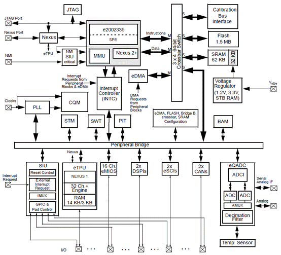
图1.MPC5634M 系列方框图 MPC5634M 系列应用: Gasoline Engine Managemen... Motorcycle Engine Control... Integrated Small Engine C... Hybrid Electric Vehicle (... Advanced Heat Meter Low-End Mechanical Type w... Controller Area Network (... Diesel Engine Management Basic Heat Meter Thermostat TRK-MPC5634M低成本开发系统 The TRK-MPC5634M is a low-cost development system supporting Freescale MPC5634M microcontrollers in 144LQFP packages. The Embedded OSJTAG circuitry on the TRK-MPC5634M board allows the processor on the board to be debugged and programmed via USB from a PC. In addition, the demo board can be powered using the USB bus. The TRK-MPC5634M package includes the following items: • TRK-MPC5634M Board • CodeWarrior Development Studio DVD-ROM • TRK-MPC5634M Resources CD • USB A-to-B Cable • Freescale Warranty Card 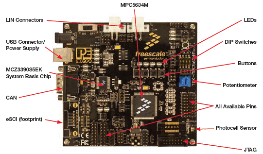
图2.TRK-MPC5604M 开发板外形图 TRK-MPC5604M 开发板主要特性: • Soldered MPC5634M LQFP144 device • Access to MCU pins with standard headers • Embedded OSJTAG: USB to JTAG circuitry which allows host PC to communicate with the microcontroller through USB 2.0. • On-board Virtual Serial Port • ON/OFF Power Switch w/ LED indicator • A 9VDC to 12VDC power supply input barrel connector • Power Input Selection Jumpers for selecting the input voltage source: • Power Input from USB Connector • Power Input from DC Power Jack • Freescale MC3390x • Jumper to select BAM source: • From internal memory • From CAN • From LIN Flex • RESET Push Button and LED indicator w/ enable • User Features: • 4 User Push Buttons w/ enable and pull-up & pull-down options • 4 DIL switches w/ enable and pull-up & pull-down options • 10K Ohm POT connected to an ADC input channel w/ enable • 1 photocell w/ enable • 4 User LED’s w/ enable • 1 RS232 interface w/ enable (DB9 and transceiver footprint only) • 1 CAN interface w/ enable to high-speed CAN transceiver with DB9 CAN connector • 2 LIN channels w/ enable sharing one LIN transceiver with two standard LIN connectors • 4 distinct GND test points • Specifications: • Board Size 4.7” x 4.3” • Power Input: • USB Cable: 5VDC, 500mA max • DC Power Jack: 2.1/5.5mm barrel connector, 9VDC to 12VDC Center Positive 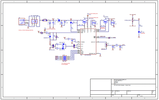
图3.TRK-MPC5604M 开发板电路图(1) 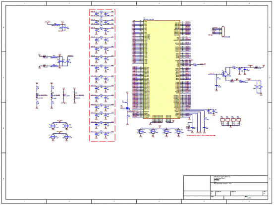
图4TRK-MPC5604M 开发板电路图(2) 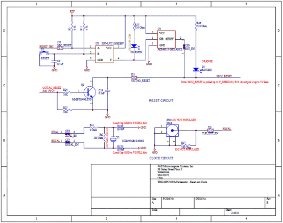
图5.TRK-MPC5604M 开发板电路图(3) 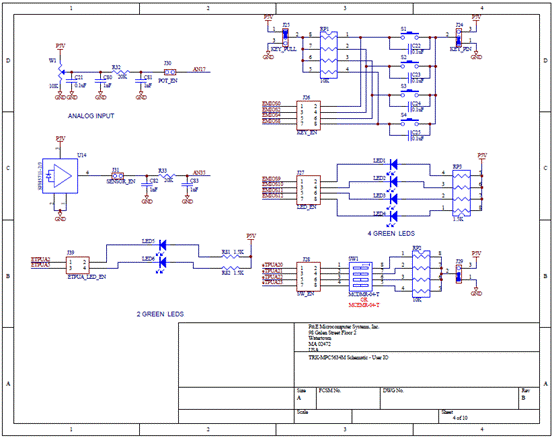
图6.TRK-MPC5604M 开发板电路图(4) 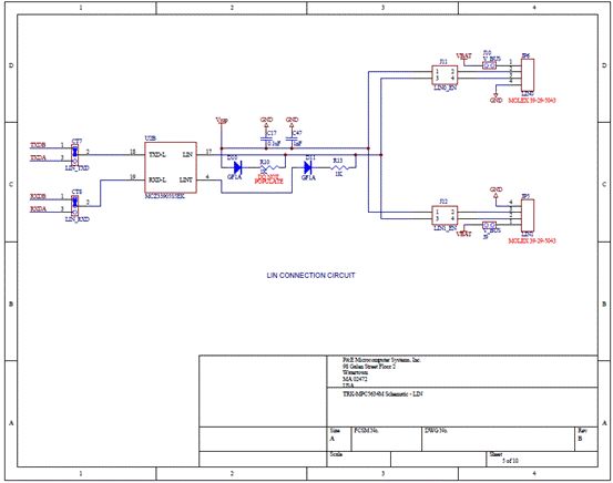
图7.TRK-MPC5604M 开发板电路图(5) 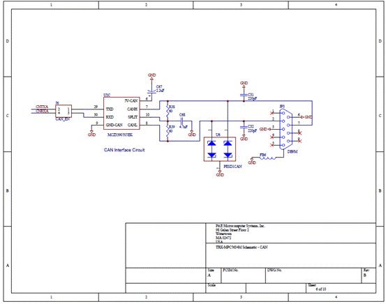
图8.TRK-MPC5604M 开发板电路图(6) 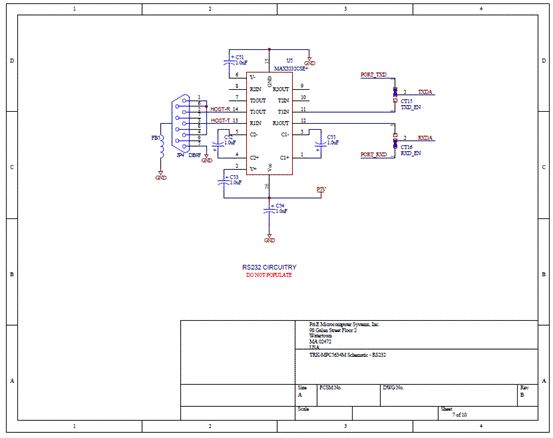
图9.TRK-MPC5604M 开发板电路图(7) 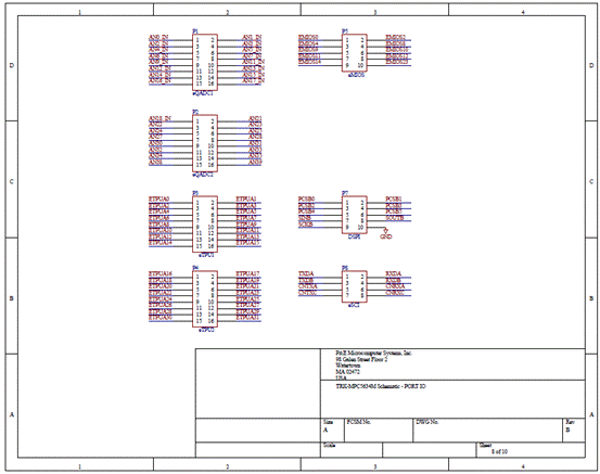
图10.TRK-MPC5604M 开发板电路图(8) 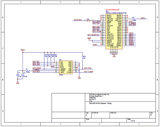
图11.TRK-MPC5604M 开发板电路图(9) 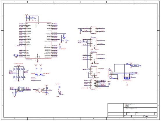
图12.TRK-MPC5604M 开发板电路图(10) 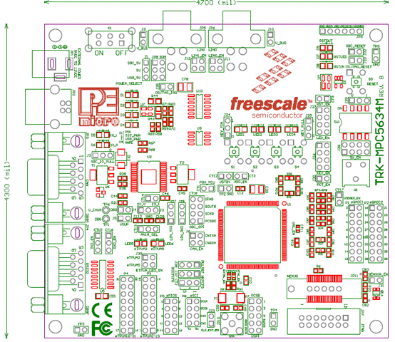
图13.TRK-MPC5604M 开发板PCB布局图(1) 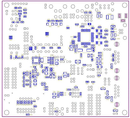
图14.TRK-MPC5604M 开发板PCB布局图(2) 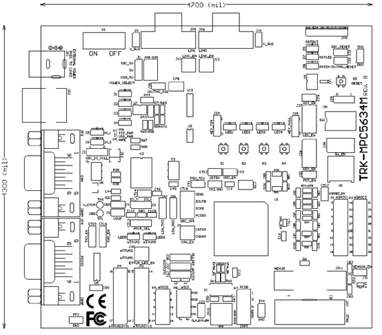
图15.TRK-MPC5604M 开发板PCB布局图(3) 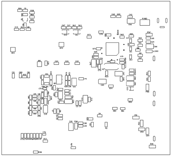
图16.TRK-MPC5604M 开发板PCB布局图(4) 详情请见:  MPC5634M.pdf
(1.28 MB)
和  TRKMPC5634MSCH.pdf
(393.5 KB)
来源:网络 |


网友评论