TI PGA450-Q1超声波汽车倒车解决方案
发布时间:2012-6-8 11:47
发布者:1770309616
|
TI 公司的PGA450-Q1是全集成超声波传感器接口器件,集成了电压稳压器,12位SAR ADC,8位微控制器,数字带通滤波器,DAC,两个NMOS低边驱动器,低噪音放大器,振荡器,LIN 2.1物理接口协议接口.主要用于汽车泊车, 盲区检测和物体检测.本文介绍了PGA450-Q1主要特性,功能方框图, 应用电路图, 评估板PGA450-Q1 EVM主要特性,电路图和PCB布局图. The PGA450-Q1 is a fully integrated interface device for ultrasonic transducers used in automotive park distance or object detection applications. It incorporates these system blocks: voltage regulators, a 12-bit SAR ADC, an 8-bit microcontroller, a digital band-pass filter, a DAC, dual NMOS low-side drivers, a low-noise amplifier, an oscillator, and a LIN 2.1 physical interface and protocol for interfacing. The PGA450-Q1 possesses an 8-bit microcontroller and OTP memory for program storage for processing the echo signal and calculating the distance between the transducer and the object. This data is transmitted through the LIN 2.1 communication protocol. The LIN 2.1 physical layer is slave-only and does not implement the LIN wake-up feature. PGA450-Q1主要特性: Dual NMOS Low-Side Drivers Configurable Burst Generator Low-Noise Amplifier 12-Bit SAR ADC Configurable Digital Band-Pass Filter Digital Signal Envelope Detect On-Chip 8-Bit Microprocessor LIN 2.1 Physical Interface and Protocol Watchdog Timer Four-Wire SPI for Testability / Programming 8K Bytes OTP 768 Bytes of FIFO RAM 256 Bytes Scratchpad RAM 8K Bytes of Development RAM 32 Bytes of EEPROM for Application PGA450-Q1应用: Automotive Park Distance Blind Spot Detection Object Detection Applications 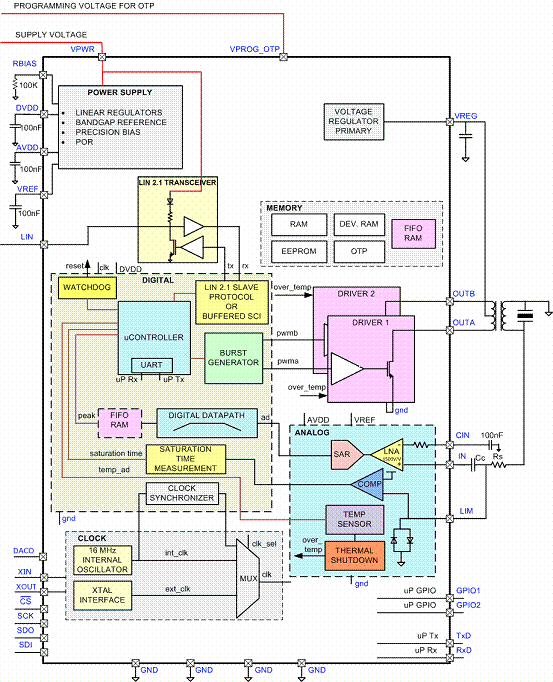
图1.PGA450-Q1功能方框图 The digital data path has the following components: • Band-pass filter • Rectifier • Peak extractor • Downsampler • Low-pass filter 
图2.PGA450-Q1数字数据通路方框图 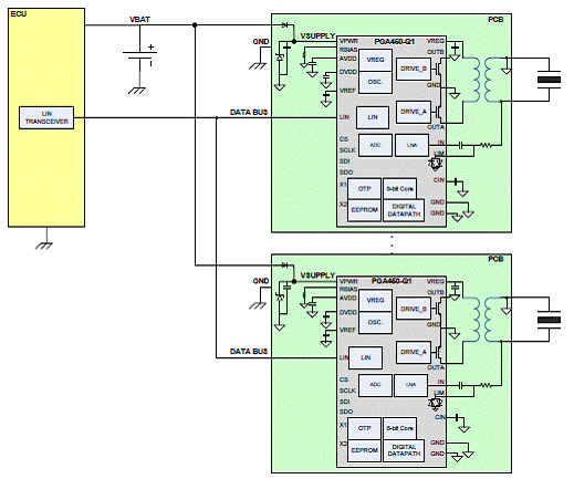
图3.PGA450-Q1应用电路图 评估板PGA450-Q1 EVM This user’s guide describes the characteristics, operation, and use of the PGA450-Q1 EVM. 评估板PGA450-Q1 EVM主要特性: • Single power-supply input for basic operation • Example single-ended transformer and 58-kHz transducer • LIN master transceiver • RS-232 transceiver for UART testing and debug • PC control with a graphical user interface and USB communications board 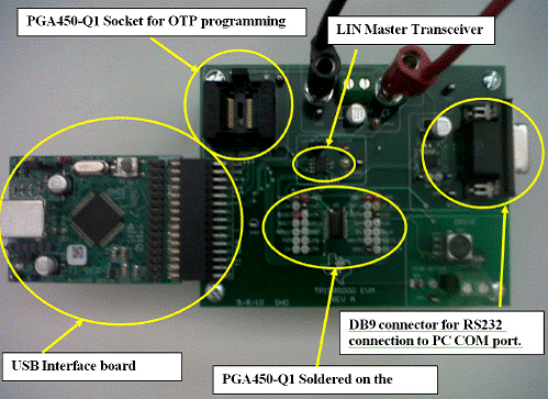
图4.评估板PGA450-Q1 EVM外形图 
图5.评估板PGA450-Q1 EVM电路图  IN IN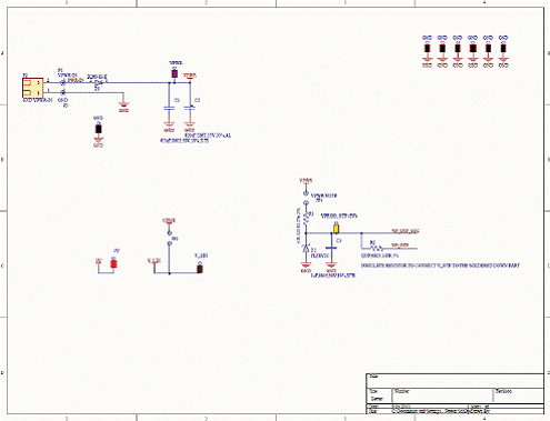
图6.评估板PGA450-Q1 EVM电路图:电源 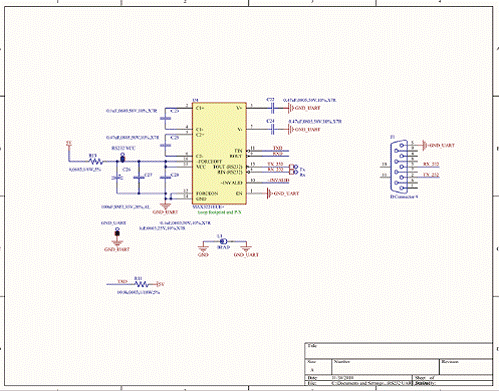
图7.评估板PGA450-Q1 EVM电路图:RS232 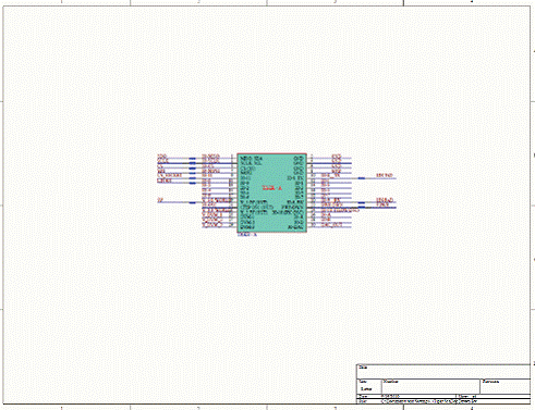
图8.评估板PGA450-Q1 EVM电路图:USB控制器 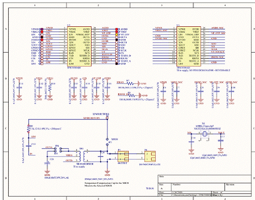
图9.评估板PGA450-Q1 EVM电路图: PGA450-Q1 
图10.评估板PGA450-Q1 EVM PCB布局图:顶层 
图11.评估板PGA450-Q1 EVM PCB布局图:底层 详情请见:  pga450-q1[1].pdf
(1.09 MB)
 sldu007[1].pdf
(4.4 MB)
来源:网络 |


网友评论