Powerint LNK460VG 100W A19 LED灯电源方案
发布时间:2012-3-30 12:29
发布者:1770309616
|
Powerint公司的DER322参考设计采用LinkSwitch-PL系列LNK460VG器件,是业界首个可替代100W A19白炽灯的LED驱动器,采用单层PCB,具有低成本少元件数和小尺寸特点,230VAC时的效率大于93%,PF大于0.9,230 VAC; 78 V LED时的THD小于20%,集成了包保护和可靠性特性,热关断自动恢复。本文介绍了LinkSwitch-PL系列产品亮点,方框图,典型应用电路以及DER322参考设计主要特性和指标,电路图,材料清单和PCB布局图。 The LinkSwitch-PL family enables a very small and low cost single-stage power factor corrected constant current driver for solid state lighting. Optimized for direct LED current sensing, the LinkSwitch-PL operates over a wide input voltage range delivering an output power of up to 16 W. The LinkSwitch-PL control algorithm provides flicker-free TRIAC dimming with minimal external components. Each device incorporates a 725 V rated power MOSFET, a novel discontinuous mode variable frequency variable on-time controller, frequency jitter, cycle by cycle current limit and hysteretic thermal shutdown in a monolithic 4-pin IC, available in SO-8C, eSOP-12, and eDIP-12 packages. LinkSwitch-PL系列产品亮点: Dramatically Simplifies Off-line LED Drivers • Flicker-free phase-controlled TRIAC dimming • Single stage power factor correction and accurate constant current (CC) output • Very low component count with small non-electrolytic bulk capacitor for compact replacement lamp designs • Compact SO8, eSOP, and eDIP packages • Completely eliminates control loop compensation Advanced Performance Features • Optimized for non-isolated flyback designs • Frequency jitter greatly reduces EMI filter size and costs • Low dissipation direct sensing of LED current Advanced Protection and Safety Features • Cycle skipping regulation for abnormally low output power to clamp peak output current delivered • 725 V integrated power MOSFET allows small bulk capacitance and maximizes power capability • Short-circuit, overload, open feedback and output overvoltage protection • Hysteretic thermal shutdown • Meets high-voltage creepage between DRAIN and all other pins both on PCB and at package EcoSmart™ - Energy Efficient • High power factor optimizes system lumen per input VA • Control algorithm balances switching and conduction losses over line and load to maintain optimum efficiency 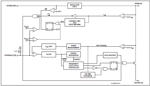
图1。LinkSwitch-PL系列功能方框图 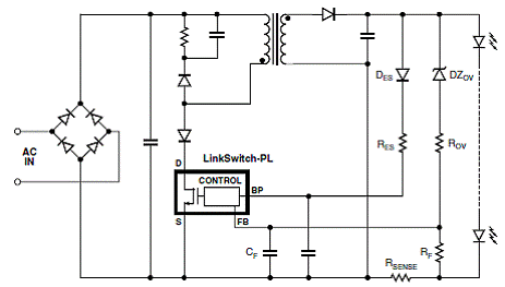
图2。LinkSwitch-PL系列典型应用电路图 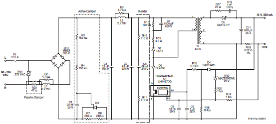
图3。采用LinkSwitch-PL系列的替代A19白炽灯的5W 15V LED驱动器电路图 DER322参考设计 High Efficiency (>93%), High Power Factor(>0.9), 18 W Output Non-Isolated Buck LED Driver Using LinkSwitchTM-PL LNK460VG The document describes a non-isolated, high efficiency, high power factor (PF) LED driver designed to drive a nominal LED string voltage of 78 V at 230 mA from an input voltage range of 195 VAC to 265 VAC (47 Hz – 63 Hz). The LED driver utilizes the LNK460VG from the LinkSwitch-PL family of ICs. The topology used is a single-stage non-isolated buck that meets the stringent space and efficiency requirements for this design. LinkSwitch-PL based designs provide high power factor (>0.9) meeting international requirements. This document contains the LED driver specification, schematic, PCB details, bill of materials, transformer documentation and typical performance characteristics. DER322参考设计主要特性: Single-stage power factor correction combined with constant current (CC) output Low cost, low component count, small size and single-sided PCB Highly energy efficient, >93% at 230 VAC input for 78 V LED Load Integrated protection and reliability features Single shot no-load protection / output short-circuit protected with auto-recovery Auto-recovering thermal shutdown with large hysteresis protects both components and PCB No damage during brown-out conditions PF >0.9 at 230 VAC % ATHD <20% at 230 VAC; 78 V LED Meets IEC ring wave, differential line surge and EN55015 conducted EMI 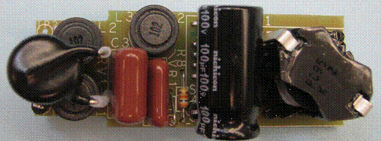
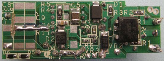
图4。DER322参考设计外形图:上:顶视图,下:底视图 DER322参考设计电源指标: 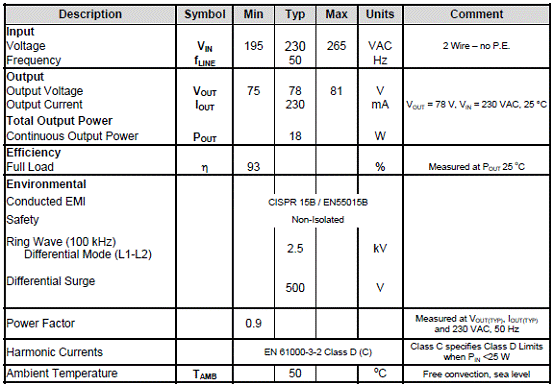
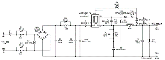
图5。DER322参考设计电路图 DER322参考设计材料清单(BOM): 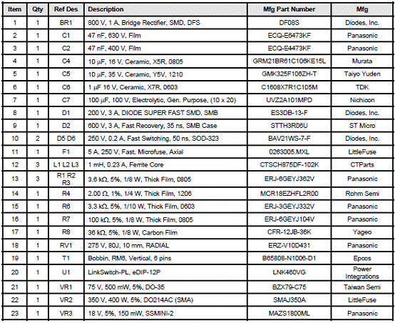
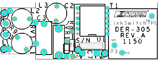
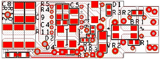
图6。DER322参考设计PCB布局图(53.5 mm x 19.6 mm):上:顶层;下:底层 详情请见:  linkswitch-pl_family_datasheet[1].pdf
(1.75 MB)
 der322[1].pdf
(4.33 MB)
来源:网络 |


网友评论