On Semi NCP1562高效350W ATX电源参考设计
发布时间:2011-10-20 13:47
发布者:1046235000
|
On Semi公司的NCP1562系列是高度集成的电压模式控制器,适用于高效率和低元件数的电源设计. NCP1562系列具有两相输出(可调重叠延时):主输出驱动正向转换器初级MOSFET,次输出驱动有源箝位电路MOSFET,次级边同步整流器,或异步半桥电路.输出电流2A,固定工作频率高达1MHz,双向频率同步,内部有100V起动电路和精密的5.0V基准,主要用在通信电源,工业电源转换器,42V汽车系统和ATX电源.本文介绍了NCP1562x系列主要特性,方框图以及高效350W ATX电源参考设计主要指标,详细电路图和相应的材料清单. The NCP1562x is a family of voltage mode controllers designed for dc--dc converters requiring high--efficiency and low parts count. These controllers incorporate two in phase outputs with an overlap delay to prevent simultaneous conduction and facilitates soft switching. The main output is designed for driving a forward converter primary MOSFET. The secondary output is designed for driving an active clamp circuit MOSFET, a synchronous rectifier on the secondary side, or an asymmetric half bridge circuit. The NCP1562 family reduces component count and system size by incorporating high accuracy on critical specifications such as maximum duty cycle limit, undervoltage detector and overcurrent threshold. Two distinctive features of the NCP1562 are soft--stop and a cycle skip current limit with a time threshold. Soft--stop circuitry powers down the converter in a controlled manner if a severe fault is detected. The cycle skip detector enables a soft--stop sequence if a continuous overcurrent condition is present. Additional features found in the NCP1562 include line feed--forward, frequency synchronization up to 1.0 MHz, cycle--by—cycle current limit with leading edge blanking (LEB), independent under and overvoltage detectors, adjustable output overlap delay, programmable maximum duty cycle, internal startup circuit and soft--start. NCP1562x系列主要特性: Dual Control Outputs with Adjustable Overlap Delay >2.0 A Output Drive Capability Soft--Stop Powers Down Converter in a Controlled Manner Cycle--by--Cycle Current Limit Cycle Skip Initiated if Continuous Current Limit Condition Exists Voltage Mode Operation with Input Voltage Feedforward Fixed Frequency Operation up to 1.0MHz Bidirectional Frequency Synchronization Independent Line Undervoltage and Overvoltage Detectors Accurate Programmable Maximum Duty Cycle Limit programmable Maximum Volt--Second Product programmable Soft--Start Internal 100 V Startup Circuit precision 5.0 V Reference These are Pb--Free Devices NCP1562x系列应用: Telecommunications Power Converters Low Output Voltage Converters using Control Driven Synchronous Rectifier Industrial Power Converters 42 V Automotive System ATX Power Supplies 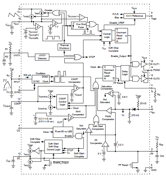
图1.NCP1562x系列方框图 高效350W ATX电源参考设计 ON Semiconductor was the first Semiconductor company to provide an 80 PLUS open reference design for an ATX Power Supply in 2005. This 1st generation reference design, was certified and met all the requirements of the 80 PLUS program. Following on this successful 1st generation design, ON Semiconductor is introducing its improved 2nd Generation reference design. This 2nd generation design utilizes newer ICs from ON Semiconductor that enable this design to exceed 80% efficiency starting at 20% load across different line conditions with ample margin to spare. This reference document provides the details behind this 2nd generation design. The design manual provides a detailed view of the performance achieved with this design in terms of efficiency, performance, thermals and other key parameters. In addition, a detailed list of the bill-of-materials (BOM) is also provided. ON Semiconductor will also be able to provide technical support to help our customers design and manufacture a similar ATX power supply customized to meet their specific requirements. The results achieved in this 2nd generation design were possible due to the use of advanced new components from ON Semiconductor. These new ICs not only speeded up the overall development cycle for this new design, but also helped achieve the high efficiencies while at the same time keeping a check on the overall cost. With the use of these new ICs, ON Semiconductor has proven again that the emerging requirements for high efficiency desktop power supplies can be met and further, can be optimized to meet specific performance vs. cost goals. This 2nd generation design consists of a single PCB designed to fit into the standard ATX enclosure along with a fan. Figure 1 below presents the overall architecture employed in this design – detailed schematics are included later in this design manual. As seen in figure 1, this design employed an Active Clamp forward topology using the new, highly integrated Active Clamp Controller IC from ON Semiconductor – NCP1562. A Continuous Conduction Mode (CCM) Power Factor Correction (PFC) IC was employed for the active PFC circuit. This IC, the NCP1653 provides an integrated, robust and costeffective PFC solution. The standby controller, NCP1027, is an optimized IC for the ATX power supply and incorporates a high-voltage MOSFET. On the secondary side, this architecture employs a post regulator approach for generating the 3.3 V output. This is an alternative approach to the traditional magnetic amplifier (Mag Amp) approach. Though ON Semiconductor believes that this post regulator approach provides the highest efficiency amongst the different means of generating these outputs in the power supply, it is important to note that if the customer desires to use a different approach, that is possible – i.e. a similar design can be developed that utilizes all the other pieces of this architecture without the post regulator and still achieve very good results. With the introduction of this 2nd generation, high-efficiency ATX Power Supply, ON Semiconductor has shown that with judicious choice of design tradeoffs, optimum performance is achieved at minimum cost. 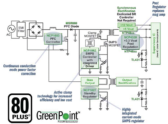
图2. ATX电源参考设计方框图 高效350W ATX电源主要指标: 
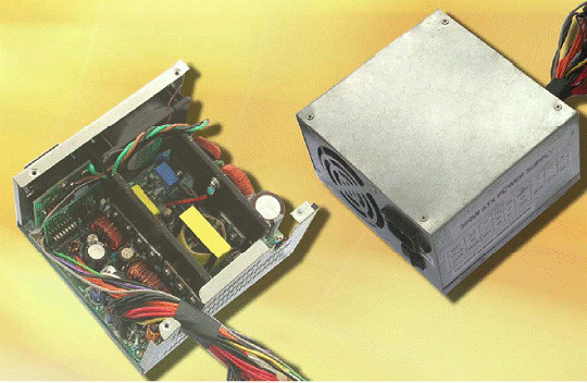
图3.350W ATX电源外形图 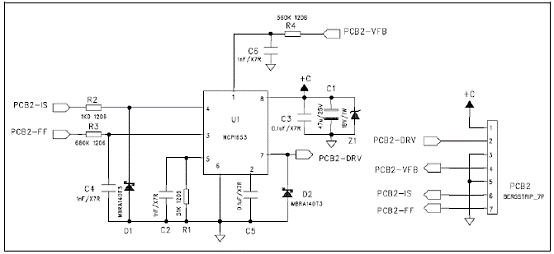
图4.PFC控制器电路图 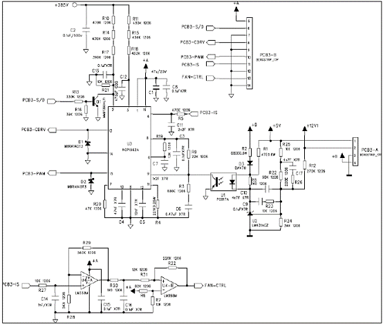
图5.EMC板电路图 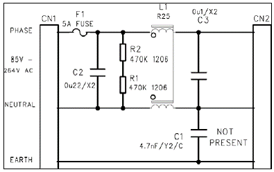
图6.有源箝位控制器板电路图 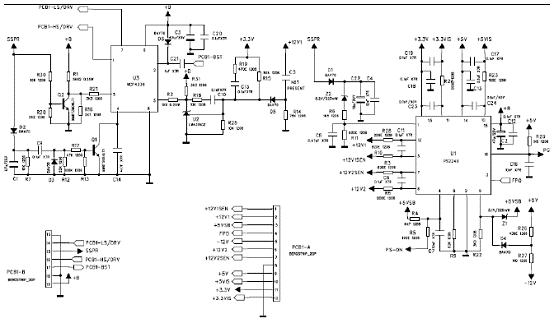
图7.监视和3.3V后稳压控制器板电路图 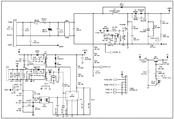
图8.主板PFC和待机部分电路图 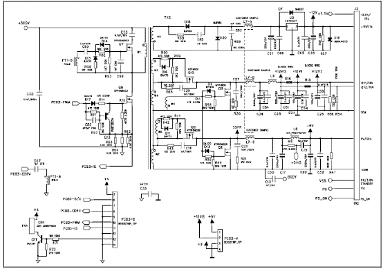
图9.主板有源箝位部分电路图 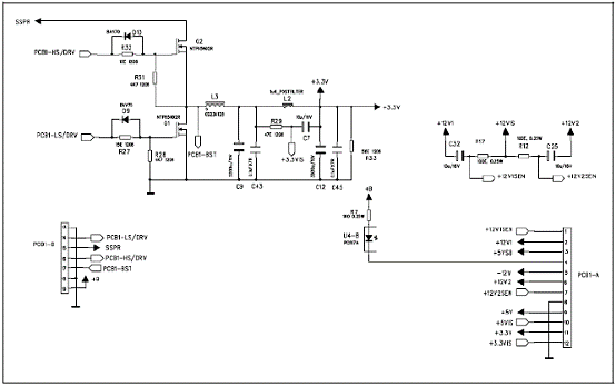
图10.主板 3.3V后稳压部分电路图 主板材料清单: 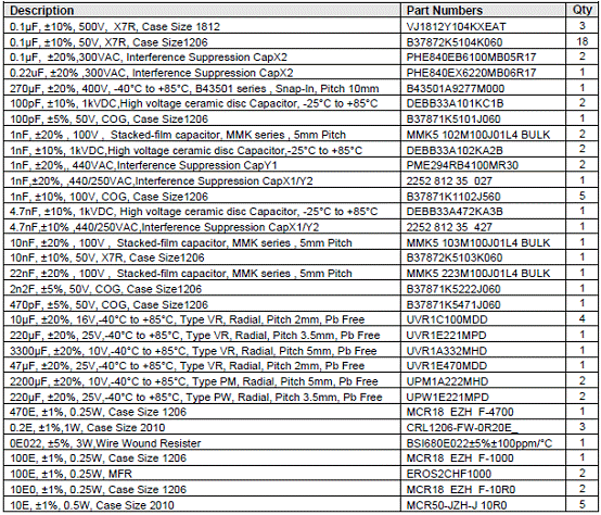
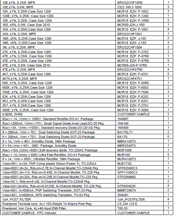
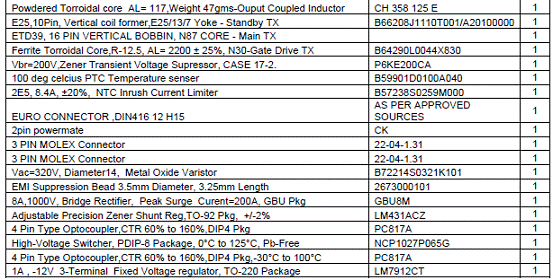
有源箝位部分材料清单: 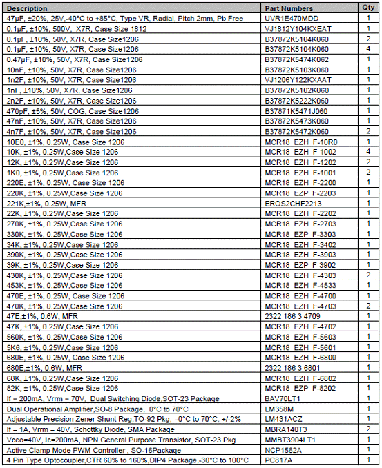
PFC部分材料清单: 
EMC部分材料清单: 
后稳压部分材料清单: 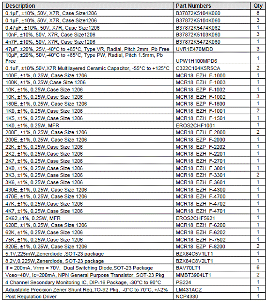
详情请见:  TND313-D[1].pdf
(633.22 KB)
|




网友评论