TI TPS84621 6A DC-DC总体电源解决方案
发布时间:2011-12-12 11:22
发布者:1046235000
|
TI 公司的TPS84621RUQ是容易使用的综合电源解决方案,集成了6A的DC/DC转换器和功率MOSFET,电感和无源元件.总体电源解决方案仅有三个外接元件,不需要回路补偿和磁性部分处理.效率大于90%,9×15×2.8 mm BQFN封装,热阻仅为13°C/W,输入电压可低至1.6V,可调开关频率250 kHz 到780 kHz,在85度C环境温度时可提供6A的额定电流,可用在宽带和通信基础设备,自动化测试和医疗设备,DSP和FPGA点负载电源,高密度分布电源系统,紧凑的PCI / PCI Express / PXI Express.本文介绍了TPS84621主要特性,功能框图,典型应用电路以及TPS84621EVM-692 6A评估模块主要特性和指标,电路图,材料清单和PCB布局图. The TPS84621RUQ is an easy-to-use integrated power solution that combines a 6-A DC/DC converter with power MOSFETs, an inductor, and passives into a low profile, BQFN package. This total power solution allows as few as 3 external components and eliminates the loop compensation and magnetics part selection process. The 9×15×2.8 mm BQFN package is easy to solder onto a printed circuit board and allows a compact point-of-load design with greater than 90% efficiency and excellent power dissipation with a thermal impedance of 13°C/W junction to ambient. The device delivers the full 6-A rated output current at 85°C ambient temperature without airflow. The TPS84621 offers the flexibility and the feature-set of a discrete point-of-load design and is ideal for powering performance DSPs and FPGAs. TPS84621主要特性: Complete Integrated Power Solution Allows Small Footprint, Low-Profile Design Efficiencies Up To 96% Wide-Output Voltage Adjust 0.6 V to 5.5 V, with 1% Reference Accuracy Optional Split Power Rail allows input voltage down to 1.6 V Adjustable Switching Frequency (250 kHz to 780 kHz) Synchronizes to an External Clock Adjustable Slow-Start Output Voltage Sequencing / Tracking Power Good Output Programmable Undervoltage Lockout (UVLO) Output Overcurrent Protection (Hiccup Mode) Over Temperature Protection Pre-bias Output Start-up Operating Temperature Range: –40°C to 85°C Enhanced Thermal Performance: 13°C/W Meets EN55022 Class B Emissions TPS84621应用: • Broadband and Communications Infrastructure • Automated Test and Medical Equipment • Compact PCI / PCI Express / PXI Express • DSP and FPGA Point of Load Applications • High Density Distributed Power Systems 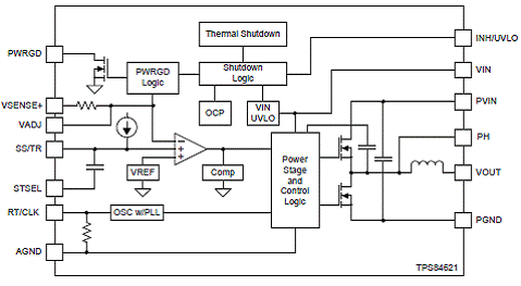
图1.TPS84621功能方框图 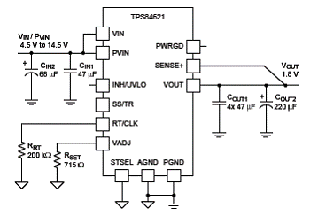
图2.TPS84621典型应用电路pVIN=VIN=4.5V-14.5V, VOUT=1.8V 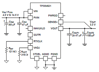
图3.TPS84621典型应用电路: PVIN = VIN = 4.5 V-14.5 V, VOUT = 3.3 V 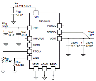
图4.TPS84621典型应用电路: PVIN=3.3 V, VIN = 4.5 V-4.5 V, VOUT =1.2 V TPS84621EVM-692 6A评估模块 The TPS84621EVM-692 is a fully assembled and tested circuit for evaluating the TPS84621 4.5-V to 14.5-V Input, 6-A Synchronous Buck, Integrated Power Solution. The TPS84621EVM-692 incorporates a DC/DC converter with output voltage and frequency that are adjustable using jumpers. This evaluation module is designed to demonstrate the small printed-circuit-board areas that may be achieved when designing with the TPS84320/620/621 regulator. The TPS84x2xEVM-692 default output voltage is 3.3 V at a 630-kHz switching frequency. The high-side and low-side MOSFETs are incorporated inside the TPS84320/620/621 package along with the gate drive circuitry. The low drain-to-source on-resistance of the MOSFET allows the TPS84320/620/621 to achieve high efficiencies and helps keep the junction temperature low at high output currents. The compensation components are internal to the TPS84320/620/621, and external resistors and jumpers allow for adjustable output voltage and frequency adjustment. Additionally, the TPS84320/620/621 provides adjustable slow start, tracking, and undervoltage lockout inputs. The absolute maximum input voltage is 15 V for the TPS84x2xEVM-692. TPS84621EVM-692主要特性: Wide-Output Voltage Adjust (0.6 V to 5.5 V), with 1% Reference Accuracy Optional Split Power Rail Allows Input Voltage Down to 1.6 V Adjustable Switching Frequency (250 kHz to 780 kHz) Synchronizes to an External Clock Adjustable Slow-Start Output Voltage Sequencing / Tracking Power Good Output Programmable Undervoltage Lockout (UVLO) Output Overcurrent Protection Over Temperature Protection Pre-bias Output Start-up TPS84621EVM-692电性能指标: 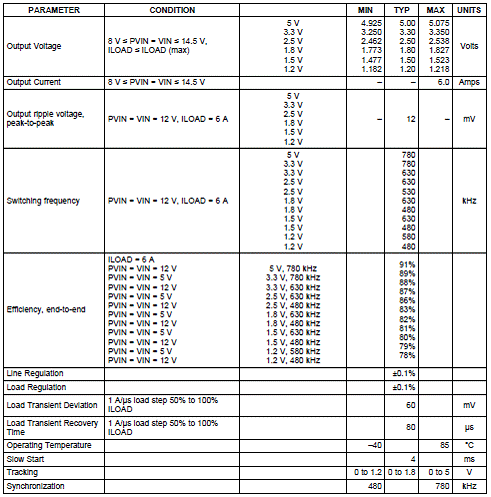
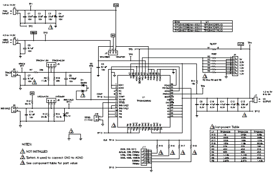
图5.TPS84x2xEVM-692电路图 TPS84621EVM-692材料清单: 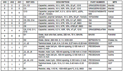
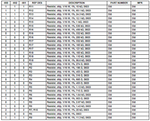
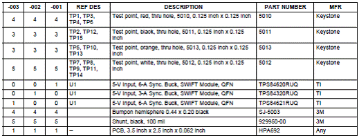
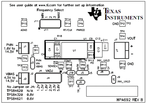
图6.TPS84x2xEVM-692 PCB布局图(顶层) 详情请见:  tps84621[1].pdf
(770.7 KB)
 sluu633[1].pdf
(367.17 KB)
|





网友评论