NXP SSL21082, TEA1721КЭJN5148вЃПи11W LEDЧ§ЖЏВЮПМЩшМЦ
ЗЂВМЪБМфЃК2012-5-9 14:03
ЗЂВМепЃК1770309616
|
NXPЙЋЫОЕФвЃПиЗЧИєРы11W LEDЧ§ЖЏВЮПМЩшМЦВЩгУSSL21082, TEA1721КЭ JN5148.ЩшМЦВЩгУНЕбЙЭиЦЫЖјВЛЬсЙЉОјдЕ,ВЩгУ2.4GHz RFвЃПиССЖШКЭПЊ/Йи.БОЮФжївЊНщЩмJN5148-001 IEEE802.15.4ЮоЯпMCUжївЊЬиад,ЗНПђЭМ,ЯрЙиЕФгІгУЖЈТЗвдМА11W LEDЧ§ЖЏЦїВЮПМЩшМЦжївЊЬиад,ЭъећЕчТЗЭМКЭЯргІВПЗжВФСЯЧхЕЅ. The JN5148-001 is an IEEE802.15.4 wireless microcontroller that provides a fully integrated solution for applications using the IEEE802.15.4 standard in the 2.4 - 2.5GHz ISM frequency band [1], including JenNet and ZigBee PRO. It includes all of the functionality required to meet the IEEE802.15.4, JenNet and ZigBee PRO specifications and has additional processor capability to run a wide range of applications including, but not limited to Smart Energy, Automatic Meter Reading, Remote Control, Home and Building Automation, Toys and Gaming. The JN5148-001 is an ultra low power, high performance wireless microcontroller targeted at JenNet and ZigBee PRO networking applications. The device features an enhanced 32-bit RISC processor offering high coding efficiency through variable width instructions, a multi-stage instruction pipeline and low power operation with programmable clock speeds. It also includes a 2.4GHz IEEE802.15.4 compliant transceiver, 128kB of ROM, 128kB of RAM, and a rich mix of analogue and digital peripherals. The large memory footprint allows the device to run both a network stack (e.g. ZigBee PRO) and an embedded application or in a co-processor mode. The operating current is below 18mA, allowing operation direct from a coin cell. Enhanced peripherals include low power pulse counters running in sleep mode designed for pulse counting in AMR applications and a unique Time of Flight ranging engine, allowing accurate location services to be implemented on wireless sensor networks. It also includes a 4-wire I2S audio interface, to interface directly to mainstream audio CODECs, as well as conventional MCU peripherals. Applications that transfer data wirelessly tend to be more complex than wired ones. Wireless protocols make stringent demands on frequencies, data formats, timing of data transfers, security and other issues. Application development must consider the requirements of the wireless network in addition to the product functionality and user interfaces. To minimise this complexity, Jennic provides a series of software libraries and interfaces that control the transceiver and peripherals of the JN5148. These libraries and interfaces remove the need for the developer to understand wireless protocols and greatly simplifies the programming complexities of power modes, interrupts and hardware functionality. The CPU of the JN5148 is a 32-bit load and store RISC processor. It has been architected for three key requirements: Low power consumption for battery powered applications High performance to implement a wireless protocol at the same time as complex applications Efficient coding of high-level languages such as C provided with the Jennic Software Developers Kit It features a linear 32-bit logical address space with unified memory architecture, accessing both code and data in the same address space. Registers for peripheral units, such as the timers, UARTs and the baseband processor are also mapped into this space. The CPU has access to a block of 15 32-bit General-Purpose (GP) registers together with a small number of special purpose registers which are used to store processor state and control interrupt handling. The contents of any GP register can be loaded from or stored to memory, while arithmetic and logical operations, shift and rotate operations, and signed and unsigned comparisons can be performed either between two registers and stored in a third, or between registers and a constant carried in the instruction. Operations between general or special-purpose registers execute in one cycle while those that access memory require a further cycle to allow the memory to respond. The instruction set manipulates 8, 16 and 32-bit data; this means that programs can use objects of these sizes very efficiently. Manipulation of 32-bit quantities is particularly useful for protocols and high-end applications allowing algorithms to be implemented in fewer instructions than on smaller word-size processors, and to execute in fewer clock cycles. In addition, the CPU supports hardware Multiply that can be used to efficiently implement algorithms needed by Digital Signal Processing applications. The instruction set is designed for the efficient implementation of high-level languages such as C. Access to fields in complex data structures is very efficient due to the provision of several addressing modes, together with the ability to be able to use any of the GP registers to contain the address of objects. Subroutine parameter passing is also made more efficient by using GP registers rather than pushing objects onto the stack. The recommended programming method for the JN5148 is by using C, which is supported by a software developer kit comprising a C compiler, linker and debugger. The CPU architecture also contains features that make the processor suitable for embedded, real-time applications. In some applications, it may be necessary to use a real-time operating system to allow multiple tasks to run on the processor. To provide protection for device-wide resources being altered by one task and affecting another, the processor can run in either supervisor or user mode, the former allowing access to all processor registers, while the latter only allows the GP registers to be manipulated. Supervisor mode is entered on reset or interrupt; tasks starting up would normally run in user mode in a RTOS environment. Embedded applications require efficient handling of external hardware events. Exception processing (including reset and interrupt handling) is enhanced by the inclusion of a number of special-purpose registers into which the PC and status register contents are copied as part of the operation of the exception hardware. This means that the essential registers for exception handling are stored in one cycle, rather than the slower method of pushing them onto the processor stack. The PC is also loaded with the vector address for the exception that occurred, allowing the handler to start executing in the next cycle. To improve power consumption a number of power-saving modes are implemented in the JN5148, described more fully in section 21 - Power Management and Sleep Modes. One of these modes is the CPU doze mode; under software control, the processor can be shut down and on an interrupt it will wake up to service the request. Additionally, it is possible under software control, to set the speed of the CPU to 4, 8, 16 or 32MHz. This feature can be used to trade-off processing power against current consumption. JN5148-001жївЊЬиад: ЪеЗЂЦїЬиад: • 2.4GHz IEEE802.15.4 compliant • Time of Flight ranging engine • 128-bit AES security processor • MAC accelerator with packet formatting, CRCs, address check, auto-acks, timers • 500 & 667kbps data rate modes • Integrated sleep oscillator for low power • On chip power regulation for 2.0V to 3.6V battery operation • Deep sleep current 100nA • Sleep current with active sleep timer 1.25ІЬA •<$0.50 external component cost •Rx current 17.5mA •Tx current 15.0mA •Receiver sensitivity -95dBm •Transmit power 2.5dBm MCUЬиад: •Low power 32-bit RISC CPU, 4 to 32MHz clock speed •Variable instruction width for high coding efficiency •Multi-stage instruction pipeline •128kB ROM and 128kB RAM for bootloaded program code & data •JTAG debug interface •4-input 12-bit ADC, 2 12-bit DACs, 2 comparators •3 application timer/counters, •2 UARTs •SPI port with 5 selects •2-wire serial interface •4-wire digital audio interface •Watchdog timer •Low power pulse counters •Up to 21 DIO Industrial temp (-40Ёц to +85Ёц) 8x8mm 56-lead Punched QFN Lead-free and RoHS compliant JN5148-001гХЪЦ: • Single chip integrates transceiver and microcontroller for wireless sensor networks • Large memory footprint to run ZigBee PRO or JenNet together with an application • Very low current solution for long battery life • Highly featured 32-bit RISC CPU for high performance and low power • System BOM is low in component count and cost • Extensive user peripherals JN5148-001гІгУ: • Robust and secure low power wireless applications • ZigBee PRO and JenNet networks • Smart metering (e.g. AMR) • Home and commercial building automation • Location Aware services ЈC e.g. Asset Tracking • Industrial systems • Telemetry • Remote Control • Toys and gaming peripherals 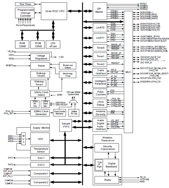
ЭМ1.JN5148-001ЗНПђЭМ 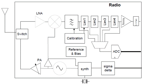
ЭМ2.JN5148-001ЮоЯпЕчМмЙЙЭМ 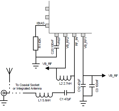
ЭМ3.JN5148-001ЭтНгЮоЯпЕчдЊМўЭМ 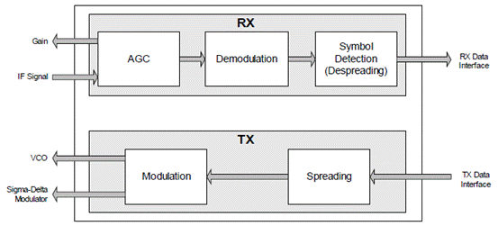
ЭМ4.JN5148-001ЕїжЦНтЕїЦїМмЙЙЭМ 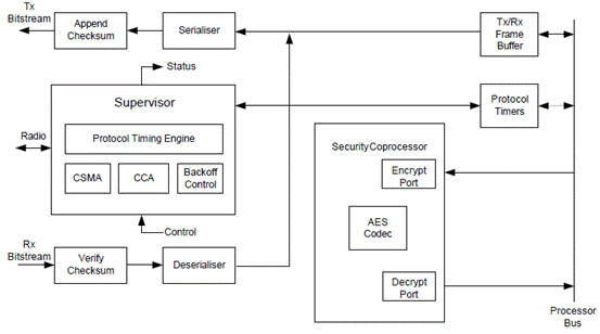
ЭМ5.JN5148-001ЛљДјДІРэЦїПђЭМ 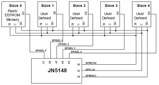
ЭМ6.JN5148-001ЕфаЭЕФSPIСЌНгЭМ ВЩгУSSL21082, TEA1721КЭJN5148ЕФвЃПиЗЧИєРы11W LEDЧ§ЖЏЦїВЮПМЩшМЦ This application note provides basic information on the operation and performance of NXP Semiconductors SSL2108X_DR1166 reference design. It contains complete remote controller 11 W SSL Driver. However, the casing with heat sink, LEDs and 2.4 GHz antenna are not included in the shipment. The design is based on buck topology which does not provide galvanic isolation. Using the RF remote control, brightness and on/off switch are controlled. 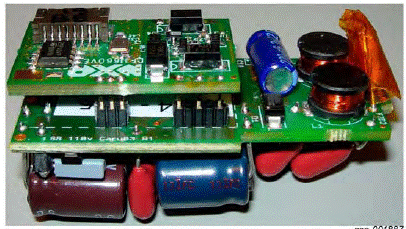
ЭМ7.120 V SSL2108XКЭDR1166бнЪОАхЭтаЮЭМ 11W LEDЧ§ЖЏЦїВЮПМЩшМЦАќРЈ: •Large signal board (SSL2108X) ЈCEMI filter ЈCMains rectifier ЈCValley fill circuit ЈCBuck inductor for supply unit ЈCSSL driver (SSL21082) •Small signal board (DR1166) buck supply (TEA1721) ЈCGenerates VCC = 2.7 V for JN5148 microcontroller/RF ЈCGenerates VDD = 13.5 V for SSL2108 driver IC •RF/microcontroller (JN5148) ЈCContains microcontroller with flash memory ЈCContains 2.4 GHz transceiver ЈCContains connector for programming the flash memory 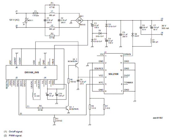
ЭМ8.11W LEDЧ§ЖЏЦїВЮПМЩшМЦЕчТЗЭМ(1) 
ЭМ9.11W LEDЧ§ЖЏЦїВЮПМЩшМЦ230VгІгУЕчТЗЭМ 
ЭМ10.ДјЧНЕїЙтЦїЕчТЗЕФSL2108xЕчТЗЭМ 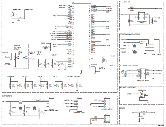
ЭМ11.DR1166КЭJN5148 RF/MCUЕчТЗЭМ 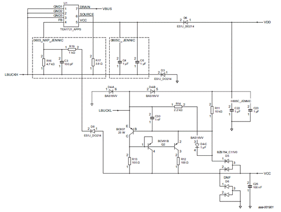
ЭМ12.DR1166КЭTEA1721НЕбЙЕчдДЕчТЗ SL2108X АхВФСЯЧхЕЅ: 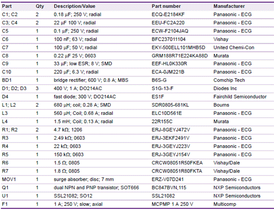
DR1166 АхВФСЯЧхЕЅ: 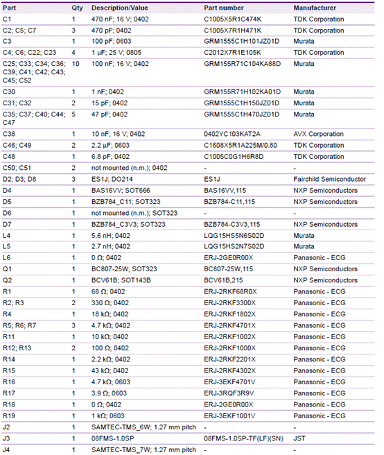

ЯъЧщЧыМћ:  JN-DS-JN5148-1v7[1].pdf
(880.93 KB)
 AN11126[1].pdf
(1.92 MB)
РДдДЃКЭјТч |




ЭјгбЦРТл