TI Stellaris LM3S2616 RDK-BDC24 BLDC马达控制方案
发布时间:2012-5-8 12:55
发布者:1770309616
|
TI 公司的Stellaris LM3S2616是基于ARM Cortex-M3内核的32位MCU,具有32位RISC性能,有多种外设如UART,CAN等,工作频率50MHz,设计用于工业应用包括遥控,电子POS机,测试和测量设备,网络设备和交换,工厂自动化,HVAC和建筑物控制,游戏设备,运动控制,医疗仪器以及消防和安全.本文介绍了 LM3S2616主要特性,方框图,RDK-BDC24 BLDC马达控制板主要特性和指标,电路图,材料清单和PCB元件布局图. The Stellaris?family of microcontrollers he first ARM?Cortex?M3 based controllers rings high-performance 32-bit computing to cost-sensitive embedded microcontroller applications. These pioneering parts deliver customers 32-bit performance at a cost equivalent to legacy 8- and 16-bit devices, all in a package with a small footprint. The Stellaris family offers efficient performance and extensive integration, favorably positioning the device into cost-conscious applications requiring significant control-processing and connectivity capabilities. The Stellaris LM3S2000 series, designed for Controller Area Network (CAN) applications, extends the Stellaris family with Bosch CAN networking technology, the golden standard in short-haul industrial networks. The Stellaris LM3S2000 series also marks the first integration of CAN capabilities with the revolutionary Cortex-M3 core. The LM3S2616 microcontroller is targeted for industrial applications, including remote monitoring, electronic point-of-sale machines, test and measurement equipment, network appliances and switches, factory automation, HVAC and building control, gaming equipment, motion control, medical instrumentation, and fire and security. For applications requiring extreme conservation of power, the LM3S2616 microcontroller features a battery-backed Hibernation module to efficiently power down the LM3S2616 to a low-power state during extended periods of inactivity. With a power-up/power-down sequencer, a continuous time counter (RTC), a pair of match registers, an APB interface to the system bus, and dedicated non-volatile memory, the Hibernation module positions the LM3S2616 microcontroller perfectly for battery applications. In addition, the LM3S2616 microcontroller offers the advantages of ARM’s widely available development tools, System-on-Chip (SoC) infrastructure IP applications, and a large user community. Additionally, the microcontroller uses ARM’s Thumb?compatible Thumb-2 instruction set to reduce memory requirements and, thereby, cost. Finally, the LM3S2616 microcontroller is code-compatible to all members of the extensive Stellaris family; providing flexibility to fit our customers’ precise needs. Texas Instruments offers a complete solution to get to market quickly, with evaluation and development boards, white papers and application notes, an easy-to-use peripheral driver library, and a strong support, sales, and distributor network. LM3S2616主要特性: The LM3S2616 microcontroller includes the following product features: ■ 32-Bit RISC Performance –32-bit ARM® Cortex™-M3 v7M architecture optimized for small-footprint embedded applications –System timer (SysTick), providing a simple, 24-bit clear-on-write, decrementing, wrap-on-zero counter with a flexible control mechanism –Thumb®-compatible Thumb-2-only instruction set processor core for high code density –50-MHz operation –Hardware-division and single-cycle-multiplication – Integrated Nested Vectored Interrupt Controller (NVIC) providing deterministic interrupt handling – 33 interrupts with eight priority levels – Memory protection unit (MPU), providing a privileged mode for protected operating system functionality – Unaligned data access, enabling data to be efficiently packed into memory – Atomic bit manipulation (bit-banding), delivering maximum memory utilization and streamlined peripheral control ■ ARM® Cortex™-M3 Processor Core –Compact core. –Thumb-2 instruction set, delivering the high-performance expected of an ARM core in the memory size usually associated with 8- and 16-bit devices; typically in the range of a few kilobytes of memory for microcontroller class applications. –Rapid application execution through Harvard architecture characterized by separate buses for instruction and data. –Exceptional interrupt handling, by implementing the register manipulations required for handling an interrupt in hardware. –Deterministic, fast interrupt processing: always 12 cycles, or just 6 cycles with tail-chaining –External non-maskable interrupt signal (NMI) available for immediate execution of NMI handler for safety critical applications. –Memory protection unit (MPU) to provide a privileged mode of operation for complex applications. –Migration from the ARM7™ processor family for better performance and power efficiency. –Full-featured debug solution •Serial Wire JTAG Debug Port (SWJ-DP) •Flash Patch and Breakpoint (FPB) unit for implementing breakpoints •Data Watchpoint and Trigger (DWT) unit for implementing watchpoints, trigger resources, and system profiling •Instrumentation Trace Macrocell (ITM) for support of printf style debugging •Trace Port Interface Unit (TPIU) for bridging to a Trace Port Analyzer –Optimized for single-cycle flash usage –Three sleep modes with clock gating for low power –Single-cycle multiply instruction and hardware divide – Atomic operations – ARM Thumb2 mixed 16-/32-bit instruction set – 1.25 DMIPS/MHz ■ JTAG –IEEE 1149.1-1990 compatible Test Access Port (TAP) controller –Four-bit Instruction Register (IR) chain for storing JTAG instructions –IEEE standard instructions: BYPASS, IDCODE, SAMPLE/PRELOAD, EXTEST and INTEST –ARM additional instructions: APACC, DPACC and ABORT –Integrated ARM Serial Wire Debug (SWD) ■ Hibernation –System power control using discrete external regulator –Dedicated pin for waking from an external signal –Low-battery detection, signaling, and interrupt generation –32-bit real-time clock (RTC) –Two 32-bit RTC match registers for timed wake-up and interrupt generation –Clock source from a 32.768-kHz external oscillator or a 4.194304-MHz crystal –RTC predivider trim for making fine adjustments to the clock rate –64 32-bit words of non-volatile memory –programmable interrupts for RTC match, external wake, and low battery events ■ Internal Memory –128 KB single-cycle flash •User-managed flash block protection on a 2-KB block basis •User-managed flash data programming •User-defined and managed flash-protection block –16 KB single-cycle SRAM –pre-programmed ROM •Stellaris family peripheral driver library (DriverLib) •Stellaris boot loader ■ DMA Controller – ARM PrimeCell® 32-channel configurable μDMA controller –Support for multiple transfer modes •Basic, for simple transfer scenarios •ping-pong, for continuous data flow to/from peripherals •Scatter-gather, from a programmable list of arbitrary transfers initiated from a single request –Dedicated channels for supported peripherals –One channel each for receive and transmit path for bidirectional peripherals –Dedicated channel for software-initiated transfers –Independently configured and operated channels –per-channel configurable bus arbitration scheme –Two levels of priority –Design optimizations for improved bus access performance between μDMA controller and the processor core •μDMA controller access is subordinate to core access •RAM striping •peripheral bus segmentation –Data sizes of 8, 16, and 32 bits –Source and destination address increment size of byte, half-word, word, or no increment –Maskable device requests –Optional software initiated requests for any channel –Interrupt on transfer completion, with a separate interrupt per channel ■ GPIOs –1-33 GPIOs, depending on configuration –5-V-tolerant in input configuration –Two means of port access: either Advanced High-Performance Bus (AHB) with better back-to-back access performance, or the legacy Advanced Peripheral Bus (APB) for backwards-compatibility with existing code –Fast toggle capable of a change every clock cycle for ports on AHB, every two clock cycles for ports on APB –programmable control for GPIO interrupts •Interrupt generation masking • Edge-triggered on rising, falling, or both • Level-sensitive on High or Low values – Bit masking in both read and write operations through address lines – Can initiate an ADC sample sequence – pins configured as digital inputs are Schmitt-triggered. – programmable control for GPIO pad configuration • Weak pull-up or pull-down resistors • 2-mA, 4-mA, and 8-mA pad drive for digital communication; up to four pads can be configured with an 18-mA pad drive for high-current applications • Slew rate control for the 8-mA drive • Open drain enables • Digital input enables ■ General-Purpose Timers –Four General-Purpose Timer Modules (GPTM), each of which provides two 16-bit timers. Each GPTM can be configured to operate independently: •As a single 32-bit timer •To trigger analog-to-digital conversions –32-bit Timer modes •programmable one-shot timer •programmable periodic timer •User-enabled stalling when the controller asserts CPU Halt flag during debug •ADC event trigger –16-bit Timer modes •General-purpose timer function with an 8-bit prescaler (for one-shot and periodic modes only) •programmable one-shot timer •programmable periodic timer •User-enabled stalling when the controller asserts CPU Halt flag during debug •ADC event trigger ■ ARM FiRM-compliant Watchdog Timer – 32-bit down counter with a programmable load register – Separate watchdog clock with an enable – programmable interrupt generation logic with interrupt masking – Lock register protection from runaway software – Reset generation logic with an enable/disable – User-enabled stalling when the controller asserts the CPU Halt flag during debug ■ ADC –Six analog input channels –Single-ended and differential-input configurations –On-chip internal temperature sensor –Sample rate of one million samples/second –Flexible, configurable analog-to-digital conversion –Four programmable sample conversion sequences from one to eight entries long, with corresponding conversion result FIFOs –Flexible trigger control •Controller (software) •Timers •Analog Comparators •pWM •GPIO –Hardware averaging of up to 64 samples for improved accuracy –Converter uses an internal 3-V reference –power and ground for the analog circuitry is separate from the digital power and ground ■ UART –Fully programmable 16C550-type UART with IrDA support –Separate 16x8 transmit (TX) and receive (RX) FIFOs to reduce CPU interrupt service loading –programmable baud-rate generator allowing speeds up to 3.125 Mbps –programmable FIFO length, including 1-byte deep operation providing conventional double-buffered interface –FIFO trigger levels of 1/8, 1/4, 1/2, 3/4, and 7/8 Standard asynchronous communication bits for start, stop, and parity – Line-break generation and detection – Fully programmable serial interface characteristics • 5, 6, 7, or 8 data bits • Even, odd, stick, or no-parity bit generation/detection • 1 or 2 stop bit generation – IrDA serial-IR (SIR) encoder/decoder providing • programmable use of IrDA Serial Infrared (SIR) or UART input/output • Support of IrDA SIR encoder/decoder functions for data rates up to 115.2 Kbps half-duplex • Support of normal 3/16 and low-power (1.41-2.23 μs) bit durations •programmable internal clock generator enabling division of reference clock by 1 to 256 for low-power mode bit duration –Dedicated Direct Memory Access (DMA) transmit and receive channels ■ I2C –Devices on the I2C bus can be designated as either a master or a slave •Supports both sending and receiving data as either a master or a slave •Supports simultaneous master and slave operation –Four I2C modes •Master transmit •Master receive •Slave transmit •Slave receive –Two transmission speeds: Standard (100 Kbps) and Fast (400 Kbps) –Master and slave interrupt generation •Master generates interrupts when a transmit or receive operation completes (or aborts due to an error) •Slave generates interrupts when data has been sent or requested by a master –Master with arbitration and clock synchronization, multimaster support, and 7-bit addressing mode ■ Controller Area Network (CAN) – CAN protocol version 2.0 part A/B – Bit rates up to 1 Mbps – 32 message objects with individual identifier masks – Maskable interrupt – Disable Automatic Retransmission mode for Time-Triggered CAN (TTCAN) applications – Programmable Loopback mode for self-test operation – programmable FIFO mode enables storage of multiple message objects – Gluelessly attaches to an external CAN interface through the CANnTX and CANnRX signals ■ Analog Comparators –Two independent integrated analog comparators –Configurable for output to drive an output pin, generate an interrupt, or initiate an ADC sample sequence –Compare external pin input to external pin input or to internal programmable voltage reference –Compare a test voltage against any one of these voltages •An individual external reference voltage •A shared single external reference voltage •A shared internal reference voltage ■ pWM –Three PWM generator blocks, each with one 16-bit counter, two PWM comparators, a PWM signal generator, a dead-band generator, and an interrupt/ADC-trigger selector –One fault input in hardware to promote low-latency shutdown –One 16-bit counter •Runs in Down or Up/Down mode •Output frequency controlled by a 16-bit load value •Load value updates can be synchronized •produces output signals at zero and load value –Two PWM comparators •Comparator value updates can be synchronized •produces output signals on match –pWM generator • Output PWM signal is constructed based on actions taken as a result of the counter and PWM comparator output signals • produces two independent PWM signals Dead-band generator • produces two PWM signals with programmable dead-band delays suitable for driving a half-H bridge • Can be bypassed, leaving input PWM signals unmodified Flexible output control block with PWM output enable of each PWM signal • pWM output enable of each PWM signal • Optional output inversion of each PWM signal (polarity control) • Optional fault handling for each PWM signal • Synchronization of timers in the PWM generator blocks • Extended PWM synchronization of timer/comparator updates across the PWM generator Blocks • Interrupt status summary of the PWM generator blocks – Can initiate an ADC sample sequence ■ QEI –position integrator that tracks the encoder position –Velocity capture using built-in timer –The input frequency of the QEI inputs may be as high as 1/4 of the processor frequency (for example, 12.5 MHz for a 50-MHz system) –Interrupt generation on: •Index pulse •Velocity-timer expiration •Direction change •Quadrature error detection ■ power –On-chip Low Drop-Out (LDO) voltage regulator, with programmable output user-adjustable from 2.25 V to 2.75 V –Hibernation module handles the power-up/down 3.3 V sequencing and control for the core digital logic and analog circuits – Low-power options on controller: Sleep and Deep-sleep modes – Low-power options for peripherals: software controls shutdown of individual peripherals – 3.3-V supply brown-out detection and reporting via interrupt or reset ■ Flexible Reset Sources –power-on reset (POR) –Reset pin assertion –Brown-out (BOR) detector alerts to system power drops –Software reset –Watchdog timer reset –Internal low drop-out (LDO) regulator output goes unregulated ■ Industrial-range 64-pin RoHS-compliant LQFP package 1.2 Target Applications ■ Remote monitoring ■ Electronic point-of-sale (POS) machines ■ Test and measurement equipment ■ Network appliances and switches ■ Factory automation ■ HVAC and building control ■ Gaming equipment ■ Motion control ■ Medical instrumentation ■ Fire and security ■ power and energy ■ Transportation 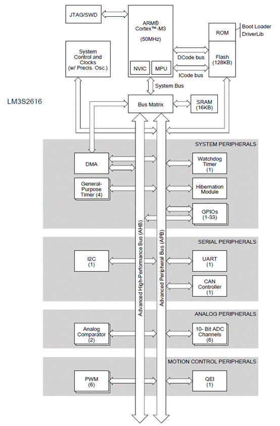
图1.Stellaris LM3S2616 MCU方框图 RDK-BDC24 BLDC马达驱动参考设计 The RDK-BDC24 is a Stellaris reference design for speed control of 12 V and 24 V brushed DC motors at up to 40 A continuous current. Features include high-performance CAN and RS232 networking as well as a rich set of control options and sensor interfaces, such as analog and quadrature encoder interfaces. High-frequency PWM enables the DC motor to run smoothly and quietly over a wide speed range. The MDL-BDC24 uses highly optimized software and a powerful 32-bit Stellaris LM3S2616 microcontroller to implement open-loop speed control as well as closed-loop control of speed, position, or motor current. The Reference Design Kit (RDK-BDC24) contains an MDL-BDC24 motor control module as well as additional hardware and software for evaluating RS232 communication. After evaluating the RDK-BDC24, users may choose to either customize parts of the hardware and software design or use the MDL-BDC24 without modification. RDK-BDC24 BLDC马达控制板主要特性: Controls brushed 12 V and 24 V DC motors up to 40 A continuous Controller Area Network (CAN) interface at 1 Mbit/s Industry-standard servo (PWM) speed input interface RS232 to CAN bridge Limit switch, encoder, and analog inputs Fully enclosed module includes cooling fan Flexible configuration options with simple source file modification Easy to customize—full source code and design files available SRDK-BDC24 BLDC马达控制板主要指标: Quiet control of brushed DC motors – 15 kHz PWM frequency Three options for Speed control – Industry-standard R-C servo type (PWM) interface – Controller Area Network (CAN) interface – RS232 serial interface CAN communication – Multicast shared serial bus for connecting systems in electromagnetically noisy Environments – 1M bits/s bit rate – CAN protocol version 2.0 A/B – Full configurability of module options – Real-time monitoring of current, voltage, speed, and other parameters – Firmware update RS232 serial communication Bridges RS232 port to a CAN network Directly interfaces to a PC serial port or National Instruments cRIO Status LED indicates Run, Direction, and Fault conditions Motor brake/coast selector Limit switch inputs for forward and reverse directions Quadrature encoder input (QEI) – Index input – 5 V supply output to encoder Analog input – Accepts 10 kΩ potentiometer or 0-3 V input Screw terminals for all power wiring Headers (0.1 inch pitch) for all control signals 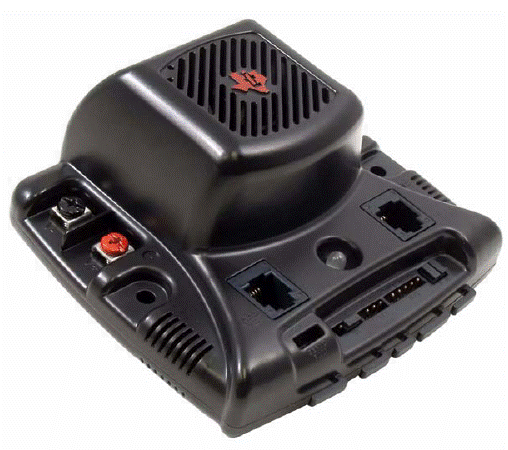
图2.MDL-BDC24 BLDC马达控制模块外形图 The RDK-BDC24 contains everything needed to evaluate brushed DC motor control. The RDK-BDC24 includes: MDL-BDC24 motor control module – Suitable for motors up to 24 V 40 A – Uses a Stellaris LM3S2616 microcontroller Mabuchi RS-555PH-3255 Brushed DC Motor – 5000 RPM, 12 V, 3 A Universal input wall power supply – 12 V 1.25 A – Plug adaptors for US, UK, EU, and AUST DB9S to 6P6C adapter – Connects the MDL-BDC24 to a PC RS232 port 6P-6C modular cable 7-ft – Use for RS232 or CAN connection CAN terminator – Plug-in 120-Ω terminator Adapter cable for ARM JTAG/SWD fine-pitch header – Texas Instruments Part ADA2 Reference design kit CD – Complete documentation, including Quickstart and user’s guides LM Flash Programmer utility for firmware updates – Complete source code, schematics, and PCB Gerber files 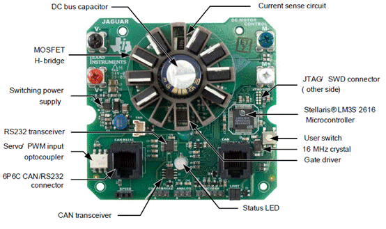
图3.MDL-BDC24 电路板外形图 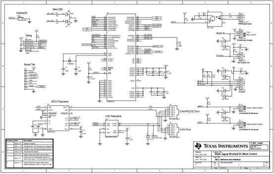
图4.MDL-BDC24 电路板电路图(1) 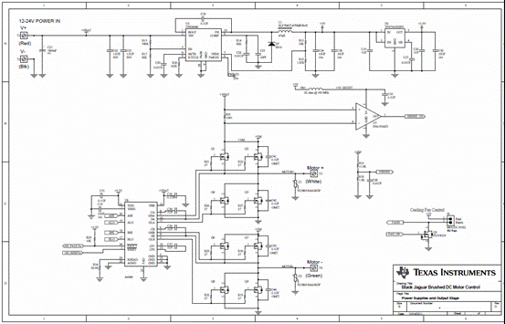
图5.MDL-BDC24 电路板电路图(2) MDL-BDC24 电路板材料清单: 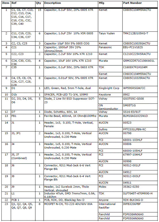
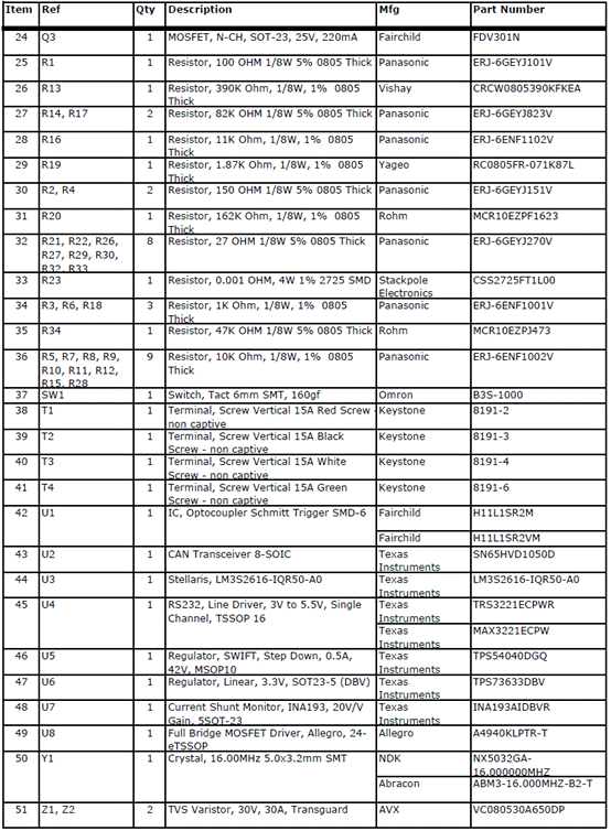
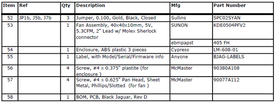
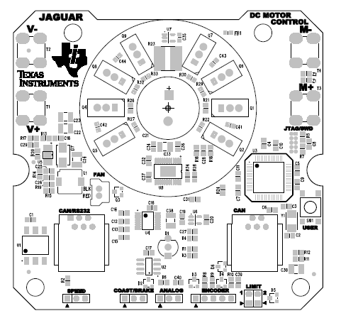
图6.MDL-BDC24 电路板PCB元件布局图 详情请见: http://www.ti.com/lit/ds/symlink/lm3s2616.pdf 和 http://www.ti.com/lit/ug/spmu130c/spmu130c.pdf |
-

-
4.12 MB, 下载积分: 积分 -1
-

-
666.32 KB, 下载积分: 积分 -1






网友评论