|
电源(power supply)
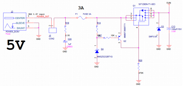
原理图(schematic) MY-I.MX6系列核心板,只需要一个5V电源(持续供电电流不低于2A,峰值2.5A-3A)输入即可。详见下图。
MY-I.MX6 series of core board only needs 5V power source(constant current is not small than 2A,peak value 2.5A-3A)as an input。details as below。
如果是直接的5V输入,5V的电源一定要做过压保护,过压保护电路参考如下。
if it is a direct 5V input,5V power source need a over voltage protection,the protection circuit can be designed with following reference。
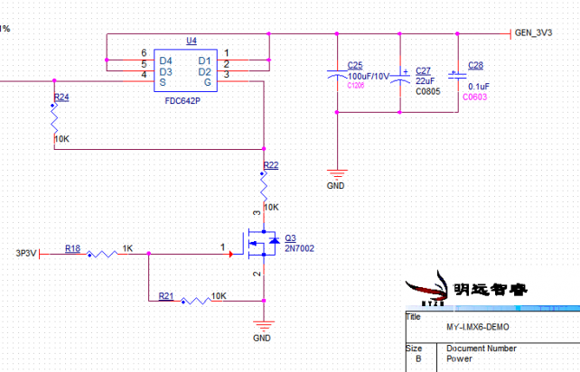
如果是高电压输入通过DCDC转换成5V,核心板会输出一个3P3V的电源,此电源的电流不超过500mA。如果底板上面3.3V的电流非常小,可以直接采用此3P3V作为底板的供电电源,如果用3P3V作为底板供电电源,请在3P3V电源上串上500mA的保险丝。
if it is high voltage input to be converted to 5V through DCDC principle,the core board will output 3P3V power source with a maximum current 500mA of which can be used as power supply for base board if current with 3.3V on the base board is too small,in this case,please put in serial a fuse for this 3P3V power source 。
由于底板上面的3.3V电压通常会超过500mA,一般用户会单独通过DCDC或者LDO产生3.3V。
since current with 3.3V on the base board is usually over 500mA,normally users will generate a another 3.3V through DCDC or LDO。
注意:底板的3.3V的电源,一定要通过核心板的3P3V来做使能控制,而不能够直接由底板上面的其他电源产生。如果底板上面还有其他电源,也必须有3P3V来做使能控制。此点是由于I.MX6芯片决定的。
note:enable control must be done for 3.3V on base board by 3P3V on core board instead of being conducted by other power sources on the base board.if there are other power sources on base board,their enable controls must be conducted by 3P3V as well,this is up to the nature of I.MX6 chip。
参考电路如下:
reference circuit as below:
PCB 核心板5V电源输入处要放置大的储能电容,确保CPU在瞬间增加负载的时候不至于断电。如果有过孔,确保过孔的电流至少能够通过3A的峰值电流,可以多打一些过孔增加电流。
capacitor with big capacity should be placed near 5V input on core board, to ensure contituous power supply even when sudden extra load is added for CPU。if there is via hole,need to make sure via hole can go through 3A peak current,more via holes can be built to increase current。
串口设计(serial port design)
原理(principle) 串口设计上面,经常会碰到的问题是RXD跟TXD的方向接反。参考原理图中的网标表示如下
for serial port design,common questions arising are inversion between RXD and TXD。network standard in the schematic as below
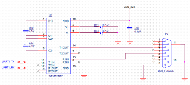
TXD——CPU输出
TXD——CPU output
RXD——CPU输入
RXD——CPU input
PCB 注意:在设计底板的时候,我司提供了底板的原理图和PCB图,串口我司采用的是母头的接口。务必确保用户在设计的时候也使用的是母头,如果要更换成公头。RS232信号要更换。公头母头的详细信息请上网查询
note:we can provide schematic and PCB diagram for design of base board,our serial port is female head as connector.please assure your design to be consistent with our offer,if change serial port to be male head connector,then RS232 siganl connector head need to be changed accordingly.For the details of male and female head connector,please get on internet for consuls.
SD卡设计(SD card design)
原理(principle) 用户在设计SD卡的时候,针对IO的上下拉,请严格参考原理图,过多的上下拉可能会导致SD卡不能够正常的工作。参考图见下面
for users'design of SD card,please follow strictly schematic to arrange IO dropdown,excessive dropdown will enable SD card not to work normally。reference diagram as below
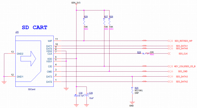
注意:如果用户不需要SD卡,要换成TF卡,由于TF卡是没有写保护这个功能的。写保护信号(SD3_RST/SD3_WP)要下拉,而不能够直接悬空。如果TF卡选用的是热插拔卡座,一定要清楚TF卡的检测管脚是哪个。一般情况是插卡之后,检测管脚接地,此时插入检测管脚(KEY_COL/SD3_CD_B)要上拉。如果TF卡选择的是翻盖式非可插拔卡座。写保护信号上拉,同时插入检测信号要接地(相当于始终插入了卡)
note:if users don't need SD card,but need TF card,since TF card doesn't have function of write-protect.Write-protect signal(SD3_RST/SD3_WP)need to pull down,which can't be hanged direclty in the air.If TF card booth is designed with hot swap,must make clear which pin of TF card is for dectetion。normally when insert the card,detection pin will be grounded,the inserted detection pin KEY_COL/SD3_CD_B)need to pull up.If TF card booth is designed with flip type,write-protect need to pull up,at the same time the inserted detection signal need to be grounded(just as a card is kept in the booth)
如果要增加ESD保护。确保接在SD_CLK信号上的ESD的电容值很小。
if need additional ESD protect,please ensure a small capacity value on SD_CLK signal。
PCBSD0,SD1,SD2,SD3,CMD,CLK信号要做等长处理。ESD原件要跟SD卡座非常接近。
SD0,SD1,SD2,SD3,CMD,CLK signal need an equal treatment。ESD originals need to be very close to SD card booth。
SATA设计(SATA design)
原理(principle) SATA的原理相对简单,确保方向正确。由于一般SATA盘的电流比较大,5V输入电流要不低于3A为好。
SATA principle is simple by contrast, only need to ensure a correct direction. since current on SATA is normally a little big, 5V current inputed is better not to be as low as 3A。

PCBSATA信号上面串联的4个电容要紧挨SATA座。
the four capacitors which are serialed to SATA signal should be close to SATA booth。
100欧姆的差分阻抗匹配
100 ohm difference resistance matching up
每组差分对之间的长度误差控制在±5mil
length tolerance for each group of differences pairs is controlled within ±5mil
要求完整参考地平面
require a full reference to ground level
HDMI
原理(principle)HDMI座子不能够接错定义
HDMI stand can't be linked with wrong definition
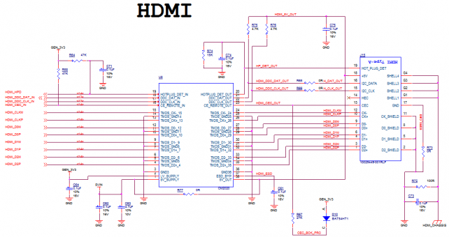
PCB100欧姆差分阻抗匹配。
100 ohm difference resistance matching up。
每组差分对之间的长度误差控制在±5mil
length tolerance for each group of differences pairs is controlled within±5mil
要求完整参考地平面
require a full reference to ground level
保护器件CM2020一定不要省略。
protect component CM2020 can't be ignored。
LVDS
原理(principle)LVDS信号如果传输距离比较远,接的屏幕比较大,LVDS信号上面可以串联耦合磁珠,能够保证传输的质量更好。
if transmitting distance for LVDS signal is long,and screen linked with is big接的屏幕比较大,amagnetic coupling can be put in serial on LVDS signal for a better transmiting quality。
PCB100欧姆的差分阻抗匹配。
100 ohm difference resistance matching up。
每组差分对之间的长度误差控制在±5mil
length tolerance for each group of differences pairs is controlled within±5mil
如果用双路LVDS信号做1080p的显示。LVDS0跟LVDS1的信号要做等长处理。
if two way LVDS singla is used for 1080p displa,。LVDS0 and LVDS1 signal need an equal treatment。
要求完整参考地平面
require a full reference to ground level
RGB接口LCD(RGB port LCD)
原理(principle)RGB接口的LCD满足24bit,18bit的接口模式
LCD as RGB port need to be matched up with interface model with 24bit,18bit
CPU信号(注1)
(CPU signal(note1)) | 24bit(注2)
(24bit(note2)) | 18bit(注3)
(18bit(note3)) | 18bit(注4)
(18bit(note4)) | | D0 | B0 | | B0 | | D1 | B1 | | B1 | | D2 | B2 | B0 | B2 | | D3 | B3 | B1 | B3 | | D4 | B4 | B2 | B4 | | D5 | B5 | B3 | B5 | | D6 | B6 | B4 | G0 | | D7 | B7 | B5 | G1 | | D8 | G0 | | G2 | | D9 | G1 | | G3 | | D10 | G2 | G0 | G4 | | D11 | G3 | G1 | G5 | | D12 | G4 | G2 | R0 | | D13 | G5 | G3 | R1 | | D14 | G6 | G4 | R2 | | D15 | G7 | G5 | R3 | | D16 | R0 | | R4 | | D17 | R1 | | R5 | | D18 | R2 | R0 | | | D19 | R3 | R1 | | | D20 | R4 | R2 | | | D21 | R5 | R3 | | | D22 | R6 | R4 | | | D23 | R7 | R5 | |
注1(note1).
D0表示CPU的液晶接口最低位,
D0 indicate a minimal level for CPU liquid crystal port,
D23表示CPU的液晶接口最高位
D23 indicate a maximal level for CPU liquid crystal port
注2(note2)
B0-24位液晶蓝色位最低位,
B0-24 bit blue bit of liquid crystal at minimal level,
B7-24位液晶蓝色位最高位
B7-24 bit blue bit of liquid crystal at maximal level,
G0-24位液晶绿色位最低位,
G0-24 bit green bit of liquid crystal at minimal level,
G7-24位液晶绿色位最高位
G7-24 bit green bit of liquid crystal at maximal level
R0-24位液晶红色位最低位,
R0-24 bit red bit of liquid crystal at minimal level,
R7-24位液晶红色位最高位
R7-24 bit red bit of liquid crystal at maximal level
注3(note3).
采用此接法,LCD软件还是选用24bit模式
in use of this kind of link,LCD software still choose 24bit model
B0-18位液晶蓝色位最低位,
B0-18 bit blue bit of liquid crystal at minimal level,
B5-18位液晶蓝色位最高位
B5-18 bit blue bit of liquid crystal at maximal level
G0-18位液晶绿色位最低位,
G0-18 bit green bit of liquid crystal at minimal level,
G5-18位液晶绿色位最高位
G5-18 bit green bit of liquid crystal at maximal level
R0-18位液晶红色位最低位,
R0-18 bit red bit of liquid crystal at minimal level,
R5-18位液晶红色位最高位
R5-18 bit red bit of liquid crystal at maximal level
注4(note 4).
采用此接法,LCD软件要改成选用18bit模式
if in use of this link method,LCD software need to choose 18bit model
B0-18位液晶蓝色位最低位,
B0-18 bit blue bit of liquid crystal at minimal level,
B5-18位液晶蓝色位最高位
B5-18 bit blue bit of liquid crystal at maximal level
G0-18位液晶绿色位最低位,
G0-18 bit green bit of liquid crystal at minimal level,
G5-18位液晶绿色位最高位
G5-18 bit green bit of liquid crystal at maximal level
R0-18位液晶红色位最低位,
R0-18 bit red bit of liquid crystal at minimal level,
R5-18位液晶红色位最高位
R5-18 bit red bit of liquid crystal at maximal level
如果静电要求非常严格,LCD信号上面要做ESD防护。
if there is a strict request with static,need ESD protect for LCD signal。
PCB所有的数据线,CLK信号要做等长处理
for all data lines,need an equal treatment for CLK signal
要求完整参考地平面
request a full reference to ground level
CMOS
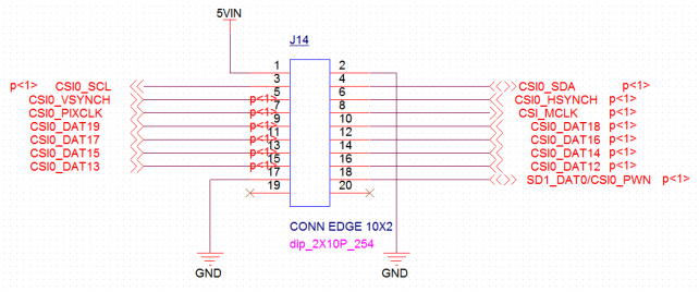
原理(principle)PCBMCLK和PIXCLK信号频率非常高,Layout时要做地隔离处理
since frequency of MCLK and PIXCLK signal is very high,need isolation treatment when Layout
数据,clk信号要做等长处理。
data,need an equal treatment for clk signal。
要求完整参考地平面
request a full reference to ground level
USB
原理(principle)USBHOST通过LAN9514扩展了4和USBHOST,同时扩展了1路10M/100M的以太网接口。
USBHOST expanded with 4 and USBHOST via LAN9514,and expanded with one way 10M/100M ethernet interface。
USB线上串耦合电感。
a coupling inductance is put in serial on USB line。
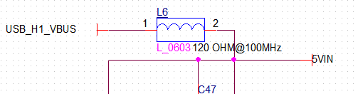
核心板的USB_H1_VBUS信号要通过磁珠接5V电源。
核心板的USB_H1_VBUS signal of coure board need to be connected with 5V power supply through magnetic bead。
对外做HOST供电时,要采用USB过流保护器件。
if power supply Host out of the board,please include over-current protect component for USD。
目前的MINIUSB口硬件设计上只能够做device口,如果要做HOST功能,请参考FSL官方的OTG设计即可。
so far only device port can be done in layout of hardware for MINIUSB port,if need function of HOST,please refer to OTG layout from FSL official。
90欧姆的差分阻抗匹配
90 ohm difference resistance matching up
要求完整参考地平面
request a full reference to ground level
对外供电的电流足够大。
current to supply outside need to be big enough。
CAN
原理(principle)由于CAN的TX,RX信号是3.3V电平,注意电平转换。
since CAN的TX,RX signal is 3.3V electrical level,attention to conversion of electrical level。
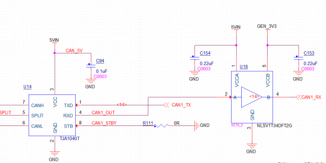
PCBCANH,CANL查分信号。
CANH,CANL check signal。
PCIE
原理(principle)TX,RX信号要串联0.1uF电容(外接模块上面如果RX信号已经串联了电容,不需要再次串联)
TX,RX signal need to connect in serial with 0.1uF capacitor(if an external module is already with a capacitor in serial,then no need to connect a capacitor again)
CLK信号上串联0.1uF电容,同时在电容后端并联一个49.9欧姆的对地电阻。
CLK signal connect in serial with 0.1uF capacitor,at the same time put a 49.8 resistor to ground in parallel with another end of the capacitor 。
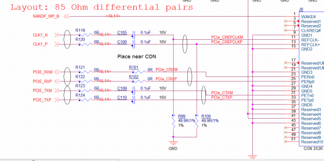
PCB85欧姆的差分阻抗匹配
85 ohm difference resistance matching up
要求完整参考地平面
request a full reference to ground level
| 


 发表于 2018-3-16 13:53:20