ADI ADuM4223 5KVrms绝缘4A输出半桥驱动器解决方案
发布时间:2012-9-21 11:41
发布者:1770309616
|
ADI公司的ADuM4223是5KVrms绝缘4A输出半桥驱动器,高边或低边相对于输入565VDC峰值,工作频率最高1MHz,CMOS输入逻辑3.3V-5V,输出驱动4.5V-18V,主要用在开关电源,绝缘IGBT/MOSFET栅极驱动和工业逆变器.本文介绍了ADuM3223/ADuM4223主要特性,功能框图,评估板EVAL-ADuM4223AEBZ主要特性,电路图,材料清单和PCB布局图. The ADuM3223/ADuM4223 provides 3000 V rms isolation in the narrow body, 16-lead SOIC package, and the ADuM4223 provides 5000 V rms isolation in the wide body, 16-lead SOIC package. Combining high speed CMOS and monolithic transformer technology, these isolation components provide outstanding performance characteristics superior to the alternatives, such as the combination of pulse transformers and gate drivers. 1 are 4 A isolated, half-bridge gate drivers that employ the Analog Devices, Inc., iCoupler® technology to provide independent and isolated high-side and low-side outputs. The ADuM3223/ADuM4223 isolators each provide two independent isolated channels. They operate with an input supply ranging from 3.0 V to 5.5 V, providing compatibility with lower voltage systems. In comparison to gate drivers employing high voltage level translation methodologies, the ADuM3223/ADuM4223 offer the benefit of true, galvanic isolation between the input and each output. Each output may be continuously operated up to 560 VPEAK relative to the input, thereby supporting low-side switching to negative voltages. The differential voltage between the high-side and low-side may be as high as 700 VPEAK. As a result, the ADuM3223/ADuM4223 provide reliable control over the switching characteristics of IGBT/MOSFET configurations over a wide range of positive or negative switching voltages. ADuM3223/ADuM4223主要特性: 4 A peak output current Working voltage High-side or low-side relative to input: 565 VDC PEAK High-side to low-side differential: 700 VDC PEAK High frequency operation: 1 MHz maximum 3.3 V to 5 V CMOS input logic 4.5 V to 18 V output drive UVLO at 2.5 V VDD1 ADuM3223A/ADuM4223A UVLO at 4.1 V VDD2 ADuM3223B/ADuM4223B UVLO at 7.0 V VDD2 ADuM3223C/ADuM4223C UVLO at 11.0 V VDD2 Precise timing characteristics 49 ns maximum isolator and driver propagation delay 5 ns maximum channel-to-channel matching CMOS input logic levels High common-mode transient immunity: >50 kV/μs Enhanced system-level ESD performance per IEC 61000-4-x High junction temperature operation: 125°C Default low output Safety and regulatory approvals (pending) ADuM3223 narrow body, 16-lead SOIC UL 1577 3000 V rms input-to-output withstand voltage ADuM4223 wide body, 16-lead SOIC UL 1577 5000 V rms input-to-output withstand voltage ADuM3223/ADuM4223应用: Switching power supplies Isolated IGBT/MOSFET gate drives Industrial inverters 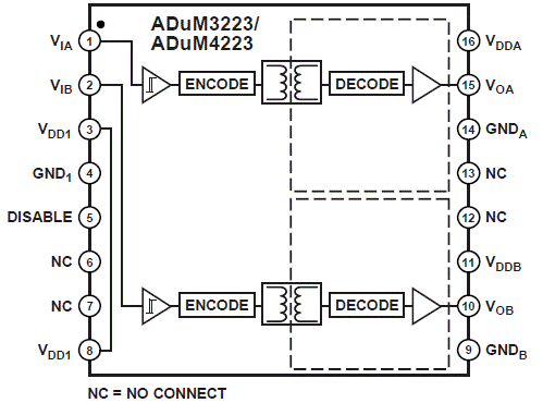
图1.ADuM3223/ADuM4223功能框图 评估板EVAL-ADuM4223AEBZ The EVAL-ADuM3223AEBZ and EVAL-ADuM4223AEBZ support the ADuM3223 and ADuM4223 isolated precision half-bridge drivers, respectively. Because the evaluation boards have footprints for IGBTs and MOSFETs in TO-263 or TO-252 packages, the ADuM3223 and ADuM4223 can be evaluated with many different power devices. The evaluation boards also allow the high-side supply to be boot-strapped to the low-side supply. The ADuM3223A model represents a superset of the ADuM3223 models because it has the lowest minimum output voltage (4.5 V). The ADuM3223B and ADuM3223C models have minimum out-put voltages of 7.5 V and 11.5 V, respectively. In the same way, the ADuM4223A model represents a superset of the ADuM4223 models. Complete information about the ADuM3223 and ADuM4223 is available in the ADuM3223/ADuM4223 data sheet, which should be consulted in conjunction with this user guide when using the evaluation board. 评估板EVAL-ADuM4223AEBZ主要特性: 4 A peak output current High frequency operation: 1 MHz maximum CMOS input logic levels 4.5 V to 18 V output drive Supports TO-263 or TO-252 IGBT/MOSFETs Bootstrap option 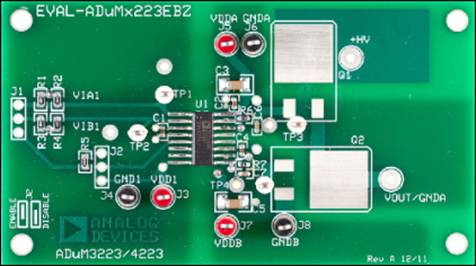
图2.ADuM3223/ADuM4223评估板外形图 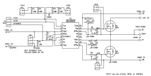
图3.ADuM3223/ADuM4223半桥驱动器电路图 ADuM3223/ADuM4223半桥驱动器材料清单: 
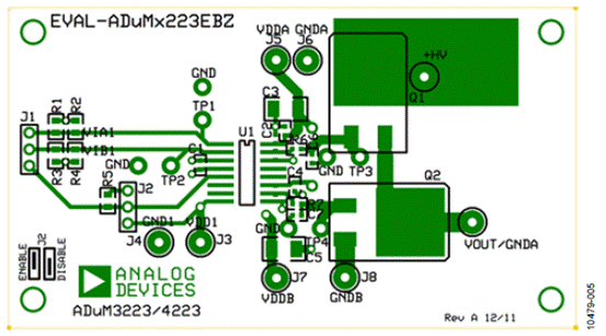
图4.ADuM3223/ADuM4223评估板PB布局图(顶层) 
图5.ADuM3223/ADuM4223评估板PB布局图(底层)  ADuM3223_4223[2].pdf
(415.65 KB)
 UG-368[2].pdf
(497.74 KB)
来源:网络 |



网友评论