
ADI AD9253四路14位125MSPS模数转换解决方案
发布时间:2012-6-5 11:21
发布者:1770309616
|
ADI公司的AD9253是集成了取样保持电路的四路14位125MSPS模数转换器(ADC),具有低成本,低功耗,体积小和容易使用的特点,工作电压1.8V,125MSPS速率时每路功耗为110mW,SNR = 74 dB ,SFDR = 90 dBc和DNL = ±0.75 LSB,满功率模拟带宽650MHz,可编程输出分辨率,主要用在超声波图像仪,高速取样,正交和多功能无线电接收器以及测试设备.本文介绍了AD9253产品亮点和主要特性,功能框图,以及AD9253CE01A评估板主要特性,电路图和材料清单. The AD9253 is a quad, 14-bit, 80 MSPS/105 MSPS/125 MSPS analog-to-digital converter (ADC) with an on-chip sample- and-hold circuit designed for low cost, low power, small size, and ease of use. The product operates at a conversion rate of up to 125 MSPS and is optimized for outstanding dynamic performance and low power in applications where a small package size is critical. The ADC requires a single 1.8 V power supply and LVPECL-/ CMOS-/LVDS-compatible sample rate clock for full performance operation. No external reference or driver components are required for many applications. The ADC automatically multiplies the sample rate clock for the appropriate LVDS serial data rate. A data clock output (DCO) for capturing data on the output and a frame clock output (FCO) for signaling a new output byte are provided. Individual-channel power-down is supported and typically consumes less than 2 mW when all channels are disabled. The ADC contains several features designed to maximize flexibility and minimize system cost, such as programmable output clock and data alignment and digital test pattern generation. The available digital test patterns include built-in deterministic and pseudorandom patterns, along with custom user-defined test patterns entered via the serial port interface (SPI). The AD9253 is available in a RoHS-compliant, 48-lead LFCSP. It is specified over the industrial temperature range of −40℃ to +85℃. This product is protected by a U.S. patent. AD9253产品亮点: Small Footprint. Four ADCs are contained in a small, space-saving package. Low power of 110 mW/channel at 125 MSPS with scalable power options. Pin compatible to the AD9633 12-bit quad ADC. Ease of Use. A data clock output (DCO) operates at frequencies of up to 500 MHz and supports double data rate (DDR) operation. User Flexibility. The SPI control offers a wide range of flexible features to meet specific system requirements. AD9253主要特性: 1.8 V supply operation Low power: 110 mW per channel at 125 MSPS with scalable power options SNR = 74 dB (to Nyquist) SFDR = 90 dBc (to Nyquist) DNL = ±0.75 LSB (typical); INL = ±2.0 LSB (typical) Serial LVDS (ANSI-644, default) and low power, reduced signal option (similar to IEEE 1596.3) 650 MHz full power analog bandwidth 2 V p-p input voltage range Serial port control Full chip and individual channel power-down modes Flexible bit orientation Built-in and custom digital test pattern generation Multichip sync and clock divider Programmable output clock and data alignment Programmable output resolution Standby mode AD9253应用: Medical ultrasound High speed imaging Quadrature radio receivers Diversity radio receivers Test equipment 
图1. AD9253功能框图 AD9253CE01A评估板 The AD9253CE01A is an evaluation board for the AD9253-125 and the AD9633-125, quad 14 and 12-bit ADCs. This reference design provides all of the support circuitry required to operate the devices in their various modes and configurations. It is designed to interface directly with the HSC-ADC-EVALC data capture card, allowing users to download captured data for analysis. The Visual Analog software package, which is used to interface with the device’s hardware, allows users to download captured data for analysis with a user-friendly graphical interface. The SPI Controller software package is also compatible with this hardware, and allows the user to access the SPI programmable features of the AD9253 and AD9633. User guide UG-328 provides documentation and instructions to configure the device for performance evaluation in the lab. (WIKI Site) The AD9253 and AD9633 data sheets provide additional information related to device configuration and performance, and should be consulted when using these tools. All documents and Visual Analog and SPI Controller are available at the High Speed ADC Evaluation Boards page. 
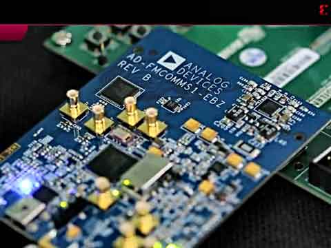
图2.AD9253CE01A评估板外形图 AD9253CE01A评估板主要特性: Full featured evaluation board for the AD9253/AD9633 SPI interface for setup and control External, on-board oscillator, or AD9517 clocking option Balun/transformer or amplifier input drive option On-board LDO regulator needing a single external 6 V, 2 A dc supply VisualAnalog® and SPI controller software interfaces 
图3.AD9253CE01A评估板电路图(1) 
图4.AD9253CE01A评估板电路图(2) 
图5.AD9253CE01A评估板电路图(3) 
图6.AD9253CE01A评估板电路图(4) 
图7.AD9253CE01A评估板电路图(5) 
图8.AD9253CE01A评估板电路图(6) 
图9.AD9253CE01A评估板电路图(7) 
图10.AD9253CE01A评估板电路图(8) 
图11.AD9253CE01A评估板电路图(9) 
图12.AD9253CE01A评估板电路图(10) AD9253CE01A评估板材料清单见: 
 AD9253CE01A评估板材料清单.rar
(10.5 KB)
AD9253CE01A评估板材料清单.rar
(10.5 KB)
详情请见:  AD9253[2].pdf
(1.24 MB)
AD9253[2].pdf
(1.24 MB)
|

网友评论