
Cypress CY8CKIT-001 PSoC3系列开发方案
发布时间:2012-2-10 11:33
发布者:1770309616
|
Cypress公司的CY8CKIT-001 PSoC3系列开发套件(DVK)是通用的开发平台,用来评估采用PSoC 1, PSoC 3或 PSoC 5架构的不同解决方案和原型,可以实现硬件,固件和软件开发. 开发套件(DVK)还包括了PSoC 1, PSoC 3或 PSoC 5系列处理器模块.本文介绍了PSoC3系列CY8C38主要特性,方框图以及CY8CKIT-001 PSoC开发套件(DVK)主要特性,开发板电路图, CY8C28系列, CY8C29系列, CY8C38系列和CY8C55系列处理器模块电路图与材料清单. With its unique array of configurable blocks, PSoC® 3 is a true system level solution providing microcontroller unit (MCU), memory, analog, and digital peripheral functions in a single chip. The CY8C38 family offers a modern method of signal acquisition, signal processing, and control with high accuracy, high bandwidth, and high flexibility. Analog capability spans the range from thermocouples (near DC voltages) to ultrasonic signals. The CY8C38 family can handle dozens of data acquisition channels and analog inputs on every general-purpose input/output (GPIO) pin. The CY8C38 family is also a high-performance configurable digital system with some part numbers including interfaces such as USB, multimaster inter-integrated circuit (I2C), and controller area network (CAN). In addition to communication interfaces, the CY8C38 family has an easy to configure logic array, flexible routing to all I/O pins, and a high-performance single cycle 8051 microprocessor core. You can easily create system-level designs using a rich library of prebuilt components and boolean primitives using PSoC Creator™, a hierarchical schematic design entry tool. The CY8C38 family provides unparalleled opportunities for analog and digital bill of materials integration while easily accommodating last minute design changes through simple firmware updates. CY8C38主要特性: Single cycle 8051 CPU DC to 67 MHz operation Multiply and divide instructions Flash program memory, up to 64 KB, 100,000 write cycles, 20 years retention, and multiple security features Up to 8-KB flash error correcting code (ECC) or configuration storage Up to 8 KB SRAM Up to 2 KB electrically erasable programmable read-only memory (EEPROM), 1 M cycles, and 20 years retention 24-channel direct memory access (DMA) with multilayer AHB[1] bus access • Programmable chained descriptors and priorities • High bandwidth 32-bit transfer support Low voltage, ultra low-power Wide operating voltage range: 0.5 V to 5.5 V High efficiency boost regulator from 0.5-V input through 1.8-V to 5.0-V output 0.8 mA at 3 MHz, 1.2 mA at 6 MHz, and 6.6 mA at 48 MHz Low-power modes including: • 1-μA sleep mode with real time clock and low-voltage detect (LVD) interrupt • 200-nA hibernate mode with RAM retention Versatile I/O system 28 to 72 I/O (62 GPIOs, eight special input/outputs (SIO), two USBIOs[2]) Any GPIO to any digital or analog peripheral routability LCD direct drive from any GPIO, up to 46 × 16 segments[2] CapSense® support from any GPIO[3] 1.2-V to 5.5-V I/O interface voltages, up to four domains Maskable, independent IRQ on any pin or port Schmitt-trigger transistor-transistor logic (TTL) inputs All GPIO configurable as open drain high/low, pull-up/pull-down, High Z, or strong output Configurable GPIO pin state at power-on reset (POR) 25 mA sink on SIO Digital peripherals 20 to 24 programmable logic device (PLD) based universal digital blocks (UDB) Full CAN 2.0b 16 Rx, 8 Tx buffers[2] Full-speed (FS) USB 2.0 12 Mbps using internal oscillator[2] Up to four 16-bit configurable timer, counter, and PWM blocks 67 MHz, 24-bit fixed point digital filter block (DFB) to implement FIR and IIR filters Library of standard peripherals • 8-, 16-, 24-, and 32-bit timers, counters, and PWMs • Serial peripheral interface (SPI), universal asynchronous transmitter receiver (UART), and I2C • Many others available in catalog Library of advanced peripherals • Cyclic redundancy check (CRC) • Pseudo random sequence (PRS) generator • Local interconnect network (LIN) bus 2.0 • Quadrature decoder Analog peripherals (1.71 V ≤ VDDA ≤ 5.5 V) 1.024 V ± 0.1% internal voltage reference across –40 °C to +85 °C Configurable delta-sigma ADC with 8- to 20-bit resolution • Sample rates up to 192 ksps • Programmable gain stage: ×0.25 to ×16 • 12-bit mode, 192 ksps, 66-dB signal to noise and distortion ratio (SINAD), ±1-bit INL/DNL • 16-bit mode, 48 ksps, 84-dB SINAD, ±2-bit INL, ±1-bit DNL Up to four 8-bit, 8-Msps IDACs or 1-Msps VDACs Four comparators with 95-ns response time Up to four uncommitted opamps with 25-mA drive capability Up to four configurable multifunction analog blocks. Example configurations are programmable gain amplifier (PGA), transimpedance amplifier (TIA), mixer, and sample and hold CapSense support Programming, debug, and trace JTAG (4-wire), serial wire debug (SWD) (2-wire), and single wire viewer (SWV) interfaces Eight address and one data breakpoint 4-KB instruction trace buffer Bootloader programming supportable through I2C, SPI, UART, USB, and other interfaces Precision, programmable clocking 3- to 62-MHz internal oscillator over full temperature and voltage range 4- to 25-MHz crystal oscillator for crystal PPM accuracy Internal PLL clock generation up to 67 MHz 32.768-kHz watch crystal oscillator Low-power internal oscillator at 1, 33, and 100 kHz Temperature and packaging –40℃ to +85 ℃ degrees industrial temperature 48-pin SSOP, 48-pin QFN, 68-pin QFN, and 100-pin TQFP package options 
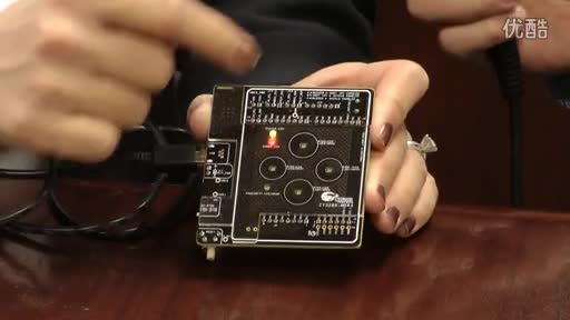
图1.CY8C38方框图 CY8CKIT-001 PSoC开发套件(DVK) The CY8CKIT-001 PSoC® Development Kit (DVK) provides a common development platform where you can prototype and evaluate different solutions using any one of the PSoC 1, PSoC 3, or PSoC 5 architectures. The PSoC DVK gives you a practical understanding of PSoC technology. In addition, the kit includes several example projects with step-by-step instructions to enable you to easily get started developing PSoC solutions. This kit includes PSoC 1, PSoC 3, and PSoC 5 Family Processor Modules. The CY8CKIT-001 PSoC Development Board is designed to aid hardware, firmware, and software developers in building their own systems around Cypress’s PSoC devices. The flexibility to configure the power domains is one of the foremost features of this board. Input power to the board is from one of two sources: ■ 12V 1A power supply adapter ■ 9V alkaline battery (not included) This full featured board incorporates three onboard linear regulators that power peripherals and PSoC processor modules at voltages between 1.7V and 5.0V. These regulators include a fixed 5V 1A linear regulator, a fixed 3.3V 300 mA linear regulator, and a 1.5V to 5.5V 300 mA adjustable regulator. The board also provides the ability to separate the PSoC core VDD rail into two separate rails, analog and digital. In addition, the board is able to separate the I/O VDD rails, giving the flexibility to power the I/O ports at different voltages. The board is equipped with a 2x16 alphanumeric LCD module capable of 1.8V to 5.0V I/O. In addition, there is a mini-B full speed USB interface and a female DB9 serial communications interface. Also included is a 12-pin wireless radio module interface which can be used to develop CyFi™ Low-Power RF or other embedded RF solutions with this kit. The board also has a prototyping area containing a small breadboard complete with I/O port sockets nearby, multipurpose LEDs, mechanical push buttons, and a multipurpose variable resistor. In addition, three capacitive sensing elements (two buttons and a five segment slider) are included on the board to allow the evaluation of CapSense® applications. The board has four GPIO expansion slots, allowing the I/O to expand to external boards. The board was designed with modularity in mind and, as a result, supports removable processor modules. This allows you to plug different PSoC processor modules into the board based upon the desired features of both 8-bit and 32-bit PSoC devices. CY8CKIT-001 PSoC开发套件(DVK)包括: ■ PSoC Development Board ■ PSoC CY8C28 Family Processor Module ■ PSoC CY8C38 Family Processor Module ■ PSoC CY8C55 Family Processor Module ■ MiniProg3 Programmer and Debug tool ■ USB Cable ■ 12V Power Supply Adapter ■ Wire Pack ■ Printed Documentation ❐ Quick Start ❐ Schematic PSoC Development Board Design ■ Software CD for PSoC 1, which includes ❐ PSoC® Designer™ IDE ❐ PSoC® Programmer™ Software ❐ CY8C28 Data Sheets ❐ Kit Release Notes ❐ Software Release Notes ❐ Example Project Files, Firmware, And Documentation ■ Software CD for PSoC 3 / PSoC 5, which includes ❐ PSoC® Creator™ IDE ❐ PSoC Programmer Software ❐ CY8C38 Data Sheet ❐ CY8C55 Data Sheet ❐ Kit Release Notes ❐ Software Release Notes ❐ Example Project Files, Firmware, And Documentation 
图2.CY8CKIT-001 PSoC开发套件(DVK)外形图 
图3.CY8CKIT-001 PSoC开发板电路图(1) 
图4.CY8CKIT-001 PSoC开发板电路图(2):CY8C28系列处理器模块 
图5.CY8CKIT-001 PSoC开发板电路图(3):CY8C29系列处理器模块 
图6.CY8CKIT-001 PSoC开发板电路图(4):CY8C38系列处理器模块 
图7.CY8CKIT-001 PSoC开发板电路图(5):CY8C55系列处理器模块 CY8CKIT-001 PSoC开发板材料清单: 

CY8C28系列处理器模块材料清单: 
CY8C29系列处理器模块材料清单: 
CY8C38系列处理器模块材料清单: 

CY8C55系列处理器模块材料清单: 

详情请见:  CY8C38xxx[1].pdf
(4.42 MB)
CY8CKIT-001 User Guide2[1].pdf
(8.42 MB)
CY8C38xxx[1].pdf
(4.42 MB)
CY8CKIT-001 User Guide2[1].pdf
(8.42 MB)
|

网友评论