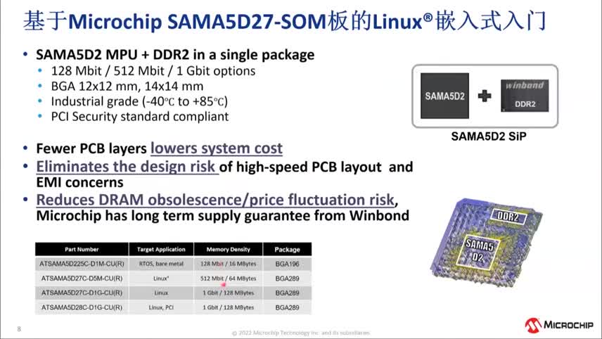
Microchip PIC18F46J50 8位无线开发解决方案
发布时间:2012-2-7 12:38
发布者:1770309616
|
Microchip公司的PIC18F46J50是采用nanoWatt XLP技术的低功耗高性能8位USB微控制器(MCU),深度睡眠模式的电流可低到13nA,工作电压2.0V-3.6V,片内集成了2.5V稳压器,具有丰富外设,主要用在智能手机,音频附属设备,视频游戏外设和先进的医疗电子.本文介绍了PIC18F46J50主要特性,方框图, 8位无线开发套件主要特性,电路图,材料清单和PCB布局图. PIC18F46J50: Low-Power, High-Performance USB Microcontrollers with nanoWatt XLP Technology This family introduces a new line of low-voltage Universal Serial Bus (USB) microcontrollers with the main traditional advantage of all PIC18 microcontrollers, namely, high computational performance and a rich feature set at an extremely competitive price point. These features make the PIC18F46J50 family a logical choice for many high-performance applications, where cost is a primary consideration. PIC18F46J50主要特性: Power Management Features with nanoWatt XLP™ for Extreme Low-Power: • Deep Sleep mode: CPU off, Peripherals off, Currents Down to 13 nA and 850 nA with RTCC: - Able to wake-up on external triggers, programmable WDT or RTCC alarm Ultra Low-Power Wake-up (ULPWU) • Sleep mode: CPU off, Peripherals off, SRAM on, Fast Wake-up, Currents Down to 105 nA, Typical • Idle: CPU off, Peripherals on, Currents Down to 2.3uA, Typical • Run: CPU on, Peripherals on, Currents Down to 6.2 uA, Typical • Timer1 Oscillator w/RTCC: 1 uA, 32 kHz, Typical • Watchdog Timer: 0.8 μA, 2V, Typical Special Microcontroller Features: • Low-Power, High-Speed CMOS Flash Technology • C Compiler Optimized Architecture for Re-Entrant Code • Priority Levels for Interrupts • Self-Programmable under Software Control • 8 x 8 Single-Cycle Hardware Multiplier • Extended Watchdog Timer (WDT): - Programmable period from 4 ms to 131s • Single-Supply In-Circuit Serial Programming™ (ICSP™) via two pins • In-Circuit Debug (ICD) w/Three Breakpoints via 2 Pins • Operating Voltage Range of 2.0V to 3.6V • On-Chip 2.5V Regulator • Flash Program Memory of 10,000 Erase/Write Cycles Minimum and 20-Year Data Retention Universal Serial Bus (USB) Features • USB V2.0 Compliant • Full Speed (12 Mbps) and Low Speed (1.5 Mbps) • Supports Control, Interrupt, Isochronous and Bulk Transfers • Supports up to 32 Endpoints (16 bidirectional) • USB module can use any RAM Location on the Device as USB Endpoint Buffers • On-Chip USB Transceiver with Crystal-less operation Flexible Oscillator Structure: • High-Precision Internal Oscillator (±0.15% typ.) for USB • Two External Clock modes, up to 48 MHz (12 MIPS) • Low-Power, 31 kHz Internal RC Oscillator • Tunable Internal Oscillator (31 kHz to 8 MHz, or up to 48 MHz with PLL) • Secondary Oscillator using Timer1 @ 32 kHz • Fail-Safe Clock Monitor: - Allows for safe shutdown if any clock stops • Two-Speed Oscillator Start-up • Programmable Reference Clock Output Generator Peripheral Highlights: • Peripheral Pin Select: - Allows independent I/O mapping of many peripherals - Continuous hardware integrity checking and safety interlocks prevent unintentional configuration changes • Hardware Real-Time Clock and Calendar (RTCC): Provides clock, calendar and alarm functions • High-Current Sink/Source 25 mA/25 mA (PORTB and PORTC) • 5.5V Tolerant Inputs (digital only pins) • Four Programmable External Interrupts • Four Input Change Interrupts • Two Enhanced Capture/Compare/PWM (ECCP) modules: - One, two or four PWM outputs - Selectable polarity - Programmable dead time - Auto-shutdown and auto-restart - Pulse steering control • Two Master Synchronous Serial Port (MSSP) modules Supporting Three-Wire SPI (all four modes) and I2C™ Master and Slave modes • Full-Duplex Master/Slave SPI DMA Engine • 8-Bit Parallel Master Port/Enhanced Parallel Slave Port • Two-Rail – Rail Analog Comparators with Input Multiplexing • 10-Bit, up to 13-Channel Analog-to-Digital (A/D) Converter module: - Auto-acquisition capability - Conversion available during Sleep - Self-calibration • High/Low-Voltage Detect module • Charge Time Measurement Unit (CTMU): - Supports capacitive touch sensing for touch screens and capacitive switches - Provides a precise resolution time measurement for both flow measurement and simple temperature sensing • Two Enhanced USART modules: - Supports RS-485, RS-232 and LIN/J2602 - Auto-Wake-up on Start bit • Auto-Baud Detect 
图1.PIC18F4XJ50 (44-PIN)方框图 8位无线开发套件 The Wireless Development Kit allows developers to evaluate and experiment with sub-GHz and 2.4 GHz RF solutions from Microchip. The Wireless Development Kit provides two RF hardware nodes which can be used to create a simple two-node wireless network. More nodes can be added by purchasing 8-Bit Wireless Development Kit or individual components. The 8-Bit Wireless Development Kit is pre-programmed with a wireless demo program that allows multiple operational configurations to be tested without writing any firmware. It also enables customer to evaluate Microchip’s proprietary wireless stacks. The Microchip wireless stacks and additional application demo source codes can be downloaded from the Microchip web site http://www.microchip.com/wireless. The PIC18 Wireless Development Board provides all the necessary components required to build an extreme low-power wireless sensor application. The Serial Accessory Port can interface external sensors or modules, like LCD Serial Accessory Board or RS232 Serial Accessory Board. The platform provides USB connectivity and supports different XLP microcontroller options. The 8-Bit Wireless Development Kit, includes either MRF24J40MA 2.4 GHz IEEE 802.15.4 complaint PICtail/PICtail Plus Daughter Boards or MRF89XAM8A 868 MHz PICtail/PICtail Plus Daughter Boards or MRF89XAM9A 915 MHz PICtail/PICtail Plus Daughter Boards. The PIC18 Wireless Development Board is compatible with many other wireless PICtail daughter Boards. 8位无线开发套件包括: The 8-Bit Wireless Development Kit contains the following items: •Two PIC18 Wireless Development Boards with PIC18F46J50 XLP Microcontroller •Two PICtail™/PICtail Plus Daughter Boards (See Table 1-1) •Two LCD Serial Accessory Boards •Two RS232 Serial Accessory Boards •Two USB A to Mini-B 1 meter Cables •Two RS232 Serial Cables 
图2.PIC18 8位无线开发板外形图 
图3.PIC18 8位无线开发板电路图(1) 
图43.PIC18 8位无线开发板电路图(2) 
图5.PIC18 8位无线开发板电路图(3) PIC18 8位无线开发板材料清单: 


图6.PIC18 8位无线开发板PCB布局图:上: 顶层,下:底层 详情请见:  39931d[1].pdf
(4.43 MB)
70654B[1].pdf
(962.85 KB)
39931d[1].pdf
(4.43 MB)
70654B[1].pdf
(962.85 KB)
来源:网络 |


网友评论