Xilinx Virtex-6 HXT FPGA ML630光传输网络评估方案
发布时间:2012-1-29 11:38
发布者:1770309616
|
Xilinx公司的Virtex-6 FPGA包括Virtex-6 LXT FPGA,Virtex-6 SXT FPGA和Virtex-6 HXT FPGA三个亚系列,采用40nm ExpressFabric和600MHz Clocking技术,具有存储器选择如能和DDR3,QDRII+和RDLRAM存储器接口,600MHz DSP48E1 Slice,高速互连性,以太网媒体接入控制器具有10/100/1000 Mbps,同时具有系统监视器和ADC,增强性配置和比特流保护,广泛用在有线通信,无线通信和广播设备。本文介绍了Virtex-6 FPGA主要特性,以及有线,无线和广播设备目标设计平台框图,ML630光传输网络(OTN)评估板主要特性和详细电路图。 Virtex-6 HXT FPGA Optical Transmission Network Evaluation Board The Virtex®-6 family provides the newest, most advanced features in the FPGA market. Virtex-6 FPGAs are the programmable silicon foundation for Targeted Design Platforms that deliver integrated software and hardware components to enable designers to focus on innovation as soon as their development cycle begins. Using the third-generation ASMBL™ (Advanced Silicon Modular Block) columnbased architecture, the Virtex-6 family contains multiple distinct sub-families. This overview covers the devices in the LXT, SXT, and HXT sub-families. Each sub-family contains a different ratio of features to most efficiently address the needs of a wide variety of advanced logic designs. In addition to the high-performance logic fabric, Virtex-6 FPGAs contain many built-in system-level blocks. These features allow logic designers to build the highest levels of performance and functionality into their FPGA-based systems. Built on a 40 nm state-of-the art copper process technology, Virtex-6 FPGAs are a programmable alternative to custom ASIC technology. Virtex-6 FPGAs offer the best solution for addressing the needs of high-performance logic designers, high-performance DSP designers, and high-performance embedded systems designers with unprecedented logic, DSP, connectivity, and soft microprocessor capabilities. Virtex-6 FPGA主要特性: • Three sub-families: • Virtex-6 LXT FPGAs: High-performance logic with advanced serial connectivity • Virtex-6 SXT FPGAs: Highest signal processing capability with advanced serial connectivity • Virtex-6 HXT FPGAs: Highest bandwidth serial connectivity • Compatibility across sub-families • LXT and SXT devices are footprint compatible in the same package • Advanced, high-performance FPGA Logic • Real 6-input look-up table (LUT) technology • Dual LUT5 (5-input LUT) option • LUT/dual flip-flop pair for applications requiring rich register mix • Improved routing efficiency • 64-bit (or two 32-bit) distributed LUT RAM option per 6-input LUT • SRL32/dual SRL16 with registered outputs option • Powerful mixed-mode clock managers (MMCM) • MMCM blocks provide zero-delay buffering, frequency synthesis, clock-phase shifting, inputjitter filtering, and phase-matched clock division • 36-Kb block RAM/FIFOs • Dual-port RAM blocks • Programmable - Dual-port widths up to 36 bits - Simple dual-port widths up to 72 bits • Enhanced programmable FIFO logic • Built-in optional error-correction circuitry • Optionally use each block as two independent 18 Kb blocks • High-performance parallel SelectIO™ technology • 1.2 to 2.5V I/O operation • Source-synchronous interfacing using ChipSync™ technology • Digitally controlled impedance (DCI) active termination • Flexible fine-grained I/O banking • High-speed memory interface support with integrated write-leveling capability • Advanced DSP48E1 slices • 25 x 18, two’s complement multiplier/accumulator • Optional pipelining • New optional pre-adder to assist filtering applications • Optional bitwise logic functionality • Dedicated cascade connections • Flexible configuration options • SPI and Parallel Flash interface • Multi-bitstream support with dedicated fallback reconfiguration logic • Automatic bus width detection • System Monitor capability on all devices • On-chip/off-chip thermal and supply voltage monitoring • JTAG access to all monitored quantities • Integrated interface blocks for PCI Express® designs • Compliant to the PCI Express Base Specification 2.0 • Gen1 (2.5 Gb/s) and Gen2 (5 Gb/s) support with GTX transceivers • Endpoint and Root Port capable • x1, x2, x4, or x8 lane support per block • GTX transceivers: up to 6.6 Gb/s • Data rates below 480 Mb/s supported by oversampling in FPGA logic. • GTH transceivers: 2.488 Gb/s to beyond 11 Gb/s • Integrated 10/100/1000 Mb/s Ethernet MAC block • Supports 1000BASE-X PCS/PMA and SGMII using GTX transceivers • Supports MII, GMII, and RGMII using SelectIO technology resources • 2500Mb/s support available • 40 nm copper CMOS process technology • 1.0V core voltage (-1, -2, -3 speed grades only) • Lower-power 0.9V core voltage option (-1L speed grade only) • High signal-integrity flip-chip packaging available in standard or Pb-free package options Virtex-6 FPGA主要器件表: 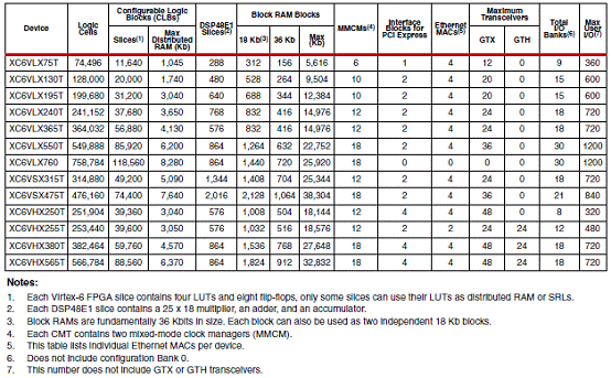
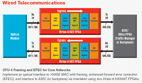
图1。有线目标设计平台框图 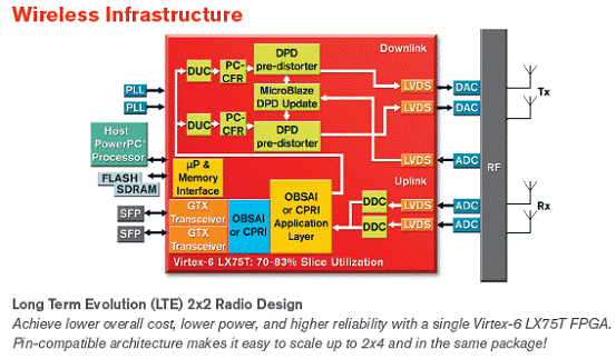
图2。无线基础设备目标设计平台框图 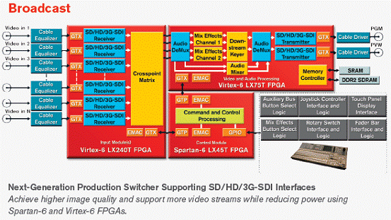
图3。广播设备目标设计平台框图 ML630 Virtex-6 HXT FPGA光传输网络(OTN)评估板 ML630 Virtex-6 HXT FPGA Optical Transmission Network(OTN)Evaluation Board This chapter describes the components, features, and operation of the ML630 Virtex®-6 HXT FPGA Optical Transmission Network (OTN) evaluation board. The ML630 board provides the hardware environment for characterizing and evaluating the GTX and GTH transceivers available on the Virtex -6 XC6VHX565T-2FFG1924C FPGA. ML630光传输网络(OTN)评估板主要特性: • Two Virtex-6 XC6VHX565T-2FFG1924C FPGAs • On-board power regulators for all necessary voltages with power status LEDs • All ML630 FPGA U1 and U2 I/O banks VCCO voltage is 2.5V • Two types of external power supply jacks (12V “brick” DIN4 type, PC ATX type) • USB JTAG configuration port for use with USB A-to-Mini-B cable • System ACE™ controller with companion CompactFlash socket • General purpose pushbutton and DIP switches, LEDs, and test I/O header for each FPGA • VGA 2X5 male debug header for each FPGA • USB-to-UART bridge with USB Mini-B pcb connector for each FPGA • Two VITA 57.1 FMC HPC connectors • I2C bus hosting EEPROM, clock sources and FMC connectors • A separate SiTime fixed 200 MHz 2.5V LVDS oscillator wired to each FPGAs global clock inputs • Eight pairs of differential clock input SMA connectors • Six I2C programmable Silicon Labs Si570 3.3V LVPECL 10 MHz to 810 MHz oscillators • Two differential input 8X8 crosspoint switches providing 16 selectable differential clock sources • Four sets of plug and receptacle FCI Airmax 120 pin connectors implementing the Interlaken interconnect protocol 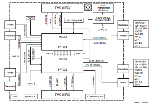
图4。ML630光传输网络(OTN)方框图 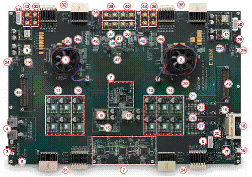
图5。ML630光传输网络(OTN)外形图 Virtex-6 HXT FPGA ML630 OTN电路图见: 
 Virtex-6 HXT FPGA ML630 OTN电路图.rar
(1.32 MB)
Virtex-6 HXT FPGA ML630 OTN材料清单见: 
 Virtex-6 HXT FPGA ML630 OTN材料清单.pdf
(80.27 KB)
详情请见:  ds150[1].pdf
(382.74 KB)
|
-

-
3.48 MB, 下载积分: 积分 -1



网友评论