ADI ADP1876 25A双路降压电源解决方案
发布时间:2011-12-5 11:57
发布者:1770309616
|
ADI公司的ADP1876是双路输出DC/DC同步降压控制器,工作频率600kHz,并集成了可驱动N-沟功率MOSFET的驱动器,输入电压2.75V-20V,功率级输入电压1V-20V,输出电压从0.6V到输入电压的90%,每路的输出电压大于25A,基准电压在−40℃到 +85℃的精度为±0.85%,主要用在消费类电子,电讯基站和网络设备以及工业和仪表.本文介绍了ADP1876主要特性,功能框图,典型应用电路和评估板ADP1876-EVALZ主要特性,电路图,材料清单和PCB布局图. The ADP1876 is a dual output dc-to-dc synchronous buck controller operating at 600 kHz fixed frequency with integrated drivers that drive N-channel power MOSFETs. An additional fixed voltage output, 150 mA linear regulator is available for powering low power loads. The device operates in current mode for improved transient response and uses valley current sensing for enhanced noise immunity. The two PWM outputs are phase shifted 180° for reducing the input current ripple and the required input capacitance. The ADP1876 provides high speed, high peak current drive capability with dead time optimization to enable energy efficient power conversion. ADP1876主要特性: Wide input range: 2.75 V to 20 V Power stage input voltage: 1 V to 20 V Output voltage range: 0.6 V up to 90% VIN Linear dropout (LDO) regulator with a fixed output 1.5 V at 150 mA Output current more than 25 A per channel 180º phase shift between channels for reduced input capacitance ±0.85% reference voltage accuracy from −40℃ to +85℃ Integrated boost diodes Independent channel precision enable Overcurrent limit protection Externally programmable soft start, slope compensation, and current sense gain Thermal overload protection Input undervoltage lockout (UVLO) Power good with internal pull-up resistor Available in 32-lead, 5 mm × 5 mm LFCSP ADP1876应用: Consumer applications Telecommunications base station and networking Industrial and instrumentation 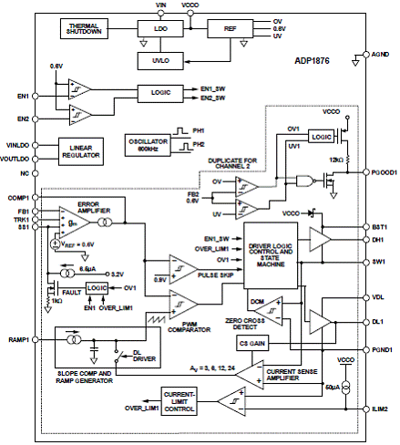
图1. ADP1876功能方框图 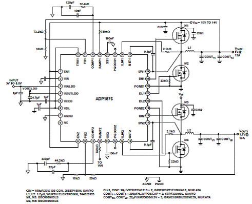
图2. ADP1876典型应用电路图 评估板ADP1876-EVALZ This user guide describes the design, operation, and test results of the ADP1876-EVALZ. The input range for this evaluation board is 10 V to 20 V, and the two regulated output voltages are set to 5 V (VOUT1) and 1.8 V (VOUT2) with a maximum 13 A output current. The power components, such as the MOFSETS, inductors, and bulk input and output capacitors, were chosen to yield a low system cost and good efficiency. 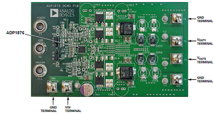
图3.评估板ADP1876-EVALZ外形图 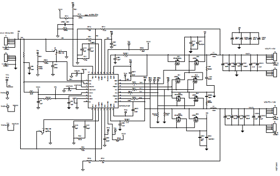
图4.评估板ADP1876-EVALZ电路图 评估板ADP1876-EVALZ材料清单: 
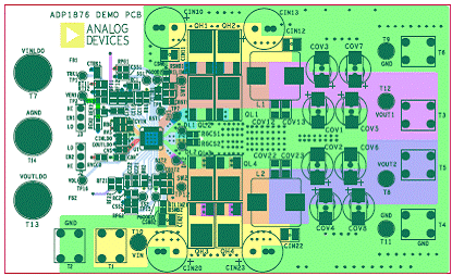
图5.评估板ADP1876-EVALZ PCB布局图 详情请见:  ADP1876.pdf
(611.92 KB)
 UG-334.pdf
(687.83 KB)
|



网友评论