
ADI AD7685ИпадФмЙ§ГЬПижЦФЃФтЧАЖЫНтОіЗНАИ
ЗЂВМЪБМфЃК2011-8-31 13:07
ЗЂВМепЃКLiming
|
ADIЙЋЫОЕФAD7685ЪЧ16ЮЛЕчКЩжиаТЗжВМж№ДЮБЦНќФЃЪ§зЊЛЛЦї(ADC),ЕЅЕчдД2.3V-5.5VЙЄзї,АќРЈгаВЛЖЊЪЇТыЕФЕЭЙІКФИпЫй16ЮЛШЁбљADC,ФкВПзЊЛЛЪБжг,вдМАЖрЙІФмДЎПк.ЭЬЭТСП250kSPS, INLЕфаЭЮЊЁР0.6 LSB,зюДѓЮЊЁР2 LSB((ЁР0.003% of FSR)),20kHzЕФSINADЮЊ93.5dB,THDЮЊ-110dB,МйадВюЗжФЃФтЪфШы,жївЊгУдкЪжГжЩшБИ,вНСЦвЧЦї,вЦЖЏЭЈаХ,PDA,Ъ§ОнВЩМЏКЭвЧЦївЧБэгкЙ§ГЬПижЦ.БОЮФНщЩмСЫAD7685жївЊЬиад, ЖрИіЕчдДгІгУЕчдДПђЭМ, еце§16ЮЛИєРыЭЌЪБШЁбљВЩМЏЯЕЭГПђЭМ,EVAL-AD76XXCB 8/10-PinЦРЙРАхжївЊЬиад,ЕчТЗЭМвдМАЭъећЕФЙ§ГЬПижЦгУИпЫйИпCMRRОЋУмФЃФтЧАЖЫМђЛЏПђЭМ, EVAL-A-INPUT-1AZЦРЙРАхЕчТЗЭМКЭВФСЯЧхЕЅ. The AD7685 is a 16-bit, charge redistribution successive approximation, analog-to-digital converter (ADC) that operates from a single power supply, VDD, between 2.3 V to 5.5 V. It contains a low power, high speed, 16-bit sampling ADC with no missing codes, an internal conversion clock, and a versatile serial interface port. The part also contains a low noise, wide bandwidth, short aperture delay, track-and-hold circuit. On the CNV rising edge, it samples an analog input IN+ between 0 V to REF with respect to a ground sense IN−. The reference voltage, REF, is applied externally and can be set up to the supply voltage. Power dissipation scales linearly with throughput. The SPI-compatible serial interface also features the ability, using the SDI input, to daisy chain several ADCs on a single 3-wire bus or provides an optional BUSY indicator. It is compatible with 1.8 V, 2.5 V, 3 V, or 5 V logic using the separate supply VIO. The AD7685 is housed in a 10-lead MSOP or a 10-lead QFN (LFCSP) with operation specified from −40ЁуC to +85ЁуC. AD7685жївЊЬиад: 16-bit resolution with no missing codes Throughput: 250 kSPS INL: ЁР0.6 LSB typical, ЁР2 LSB maximum (ЁР0.003% of FSR) SINAD: 93.5 dB @ 20 kHz THD: −110 dB @ 20 kHz Pseudo differential analog input range 0 V to VREF with VREF up to VDD No pipeline delay Single-supply operation 2.3 V to 5.5 V with 1.8 V to 5 V logic interface Serial interface SPI®-/QSPI™-/MICROWIRE™-/DSP-compatible Daisy-chain multiple ADCs, BUSY indicator Power dissipation 1.4 ІЬW @ 2.5 V/100 SPS 1.35 mW @ 2.5 V/100 kSPS, 4 mW @ 5 V/100 kSPS Standby current: 1 nA 10-lead package: MSOP (MSOP-8 size) and 3 mm ЁС 3 mm QFN (LFCSP) (SOT-23 size) Pin-for-pin-compatible with 10-lead MSOP/QFN PulSAR® ADCs AD7685гІгУ: Battery-powered equipment Medical instruments Mobile communications Personal digital assistants (PDAs) Data acquisition Instrumentation Process controls 
ЭМ1.ADCМђЛЏЕчТЗЭМ 
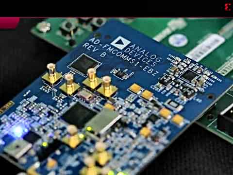
ЭМ2.AD7685 ЖрИіЕчдДгІгУЕчдДПђЭМ 
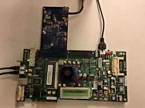
ЭМ3.AD7685еце§16ЮЛИєРыЭЌЪБШЁбљВЩМЏЯЕЭГПђЭМ EVAL-AD76XXCB 8/10-PinЦРЙРАх The EVAL-AD76XXCB 8/10-Pin is an evaluation board for the AD768x/AD769x/AD794x/AD798x 8 and 10-pin PulSAR high resolution ADCs (see the Ordering Guide at the end of this document for a product list). The evaluation board is designed to demonstrate the ADCЁЏs performance and to provide an easy to understand interface for a variety of system applications. The evaluation board is ideal for use with either Analog Devices EVAL-CONTROL BRD2/BRD3 (EVAL-CONTROL BRDx), DSP based controller board, to run the Analog devices evaluation software and to develop a specific application using LabVIEW, or as a stand-alone evaluation board. The EVAL-CONTROL BRDx is sold separately from the evaluation board, is required to run the evaluation software, is not required in stand alone mode and can be reused with many Analog Devices ADCs. EVAL-AD76XXCB 8/10-PinЦРЙРАхжївЊЬиад: Versatile analog signal conditioning circuitry On-board reference, crystal oscillator and buffers 16-bit Parallel Buffered Outputs Ideal for DSP and data acquisition card interfaces Analog and digital prototyping area for breadbording the target system Stand-alone operation or Eval control board compatibility PC software for control and data analysis LabVIEW1 driver to develop custom application 
ЭМ4. EVAL-AD76XXCB 8/10-PinЦРЙРАхЕчТЗЭМ:ФЃФтВПЗж 
ЭМ5. EVAL-AD76XXCB 8/10-PinЦРЙРАхЕчТЗЭМ:Ъ§зжВПЗж 
ЭМ6. EVAL-AD76XXCB 8/10-PinЦРЙРАхЕчТЗЭМ:ЕчдДВПЗж 
ЭМ7. EVAL-AD76XXCB 8/10-PinЦРЙРАхЕчТЗЭМ:бЁдёВПЗж ЭъећЕФЙ§ГЬПижЦгУИпЫйИпCMRRОЋУмФЃФтЧАЖЫ Complete High Speed, High CMRR Precision Analog Front End for Process Control Signal levels in industrial process control systems generally fall into one of the following categories: single-ended current (4 mA-to-20 mA), single-ended, differential voltage (0 V to 5V, 0 V to 10 V, ЁР5 V, ЁР10 V), or small signal inputs from sensors such as thermocouples or load cells. Large common-mode voltage swings are also typical, especially for small signal differential inputs; therefore good common-mode rejection is an important specification in the analog signal processing system. The analog front-end circuit shown in Figure 1 is optimized for high precision and high common-mode rejection ratio (CMRR) when processing these types of industrial-level signals. 
ЭМ8.ИпадФмЙ§ГЬПижЦЕФФЃФтЧАЖЫМђЛЏПђЭМ 
ЭМ9. EVAL-A-INPUT-1AZЦРЙРАхКЭSDPАхСЌНгЭМ 
ЭМ10. EVAL-A-INPUT-1AZЦРЙРАхЕчТЗЭМ(1) 
ЭМ11. EVAL-A-INPUT-1AZЦРЙРАхЕчТЗЭМ(2) EVAL-A-INPUT-1AZЦРЙРАхВФСЯЧхЕЅМћ: ЯъЧщЧыМћ: http://www.analog.com/static/imported-files/data_sheets/AD7685.pdf КЭ http://www.analog.com/static/imported-files/circuit_notes/CN0213.pdf |

ЭјгбЦРТл