ADI ADP2323双输出3A降压电源解决方案
发布时间:2011-7-20 17:01
发布者:Liming
|
ADI公司的ADP2323是集成了90 mΩ的高边MOSFET的双输出3A 20V同步降压电源稳压器,输入电压4.5V-20V,输出精度±1%,具有的输出配置,双路输出3A/3A,并联单输出6A,可编程开关频率250kHz到1.2MHz,主要用在通信基础设备,网络和服务器,工业和仪表,医疗保健,DC/DC POL应用等.本文介绍了ADP2323主要特性, 功能方框图,以及多种应用电路. The ADP2323 is a full featured, dual output, step-down dc-to-dc regulator based on current-mode architecture. The ADP2323 integrates two high-side power MOSFETs and two low-side drivers for the external N-channel MOSFETs. The two pulse-width mod-ulation (PWM) channels can be configured to deliver dual 3 A outputs or a parallel-to-single 6 A output. The regulator operates from input voltages of 4.5 V to 20 V, and the output voltage can be as low as 0.6 V. The switching frequency can be programmed between 250 kHz and 1.2 MHz, or synchronized to an external clock to minimize interference in multirail applications. The dual PWM channels run 180° out of phase, thereby reducing input current ripple as well as reducing the size of the input capacitor. The bidirectional synchronization pin can be programmed at a 60°, 90°, or 120° phase shift, providing the possibility for a stackable multiphase power solution. The ADP2323 can be set to operate in pulse-frequency modulation (PFM) mode at a light load for higher efficiency or in forced PWM for noise sensitive applications. External compensation and soft start provide design flexibility. Independent enable inputs and power good outputs provide reliable power sequencing. To enhance system reliability, the device also includes undervoltage lockout (UVLO), overvoltage protection (OVP), overcurrent pro-tection (OCP), and thermal shutdown (TSD). The ADP2323 operates over the −40℃ to +125℃ junction temperature range and is available in a 32-lead LFCSP_WQ package . ADP2323主要特性: Input voltage: 4.5 V to 20 V ±1% output accuracy Integrated 90 mΩ typical high-side MOSFET Flexible output configuration Dual output: 3 A/3 A Parallel single output: 6 A Programmable switching frequency: 250 kHz to 1.2 MHz External synchronization input with programmable phase shift, or internal clock output Selectable PWM or PFM mode operation Adjustable current limit for small inductor External compensation and soft start Startup into precharged output ADP2323应用: Communications infrastructure Networking and servers Industrial and instrumentation Healthcare and medical Intermediate power rail conversion DC-to-dc point of load applications 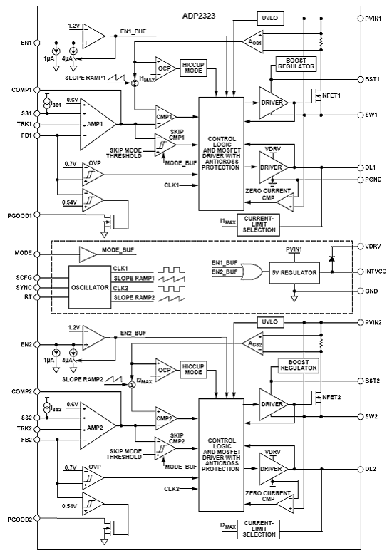
图1.ADP2323功能方框图 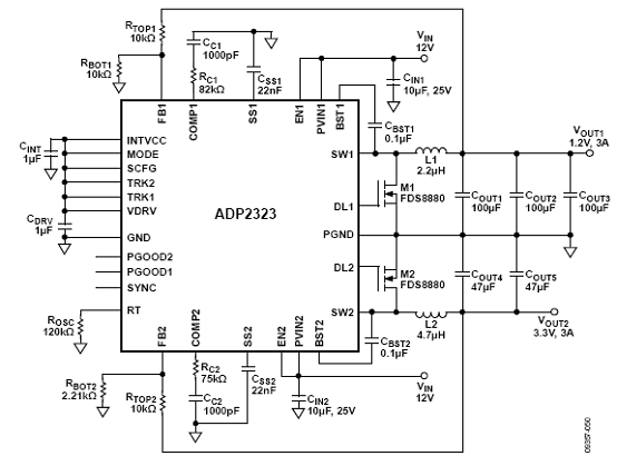
图2.ADP2323采用外接MOSFET的应用电路图: VIN1 = VIN2 = 12 V, VOUT1 = 1.2 V, IOUT1 = 3 A, VOUT2 = 3.3 V, IOUT2 = 3 A, fSW = 500 kHz 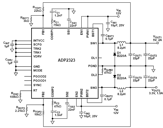
图3.ADP2323采用外接二极管的应用电路图:VIN1 = VIN2 = 12 V, VOUT1 = 5 V, IOUT1 = 2 A, VOUT2 = 3.3 V, IOUT2 = 1.5 A, fSW = 600 kHz 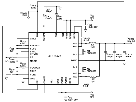
图4.ADP2323并联单输出应用电路图:IN = 12 V, VOUT = 1.8 V, IOUT = 6 A, fSW = 600 kHz 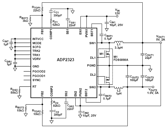
图5.ADP2323级联应用电路图: VIN1 = 12 V, VOUT1 = 5 V, IOUT1 = 2 A, VOUT2 = 1 V, IOUT2 = 3 A, fSW = 1.2 MHz 
图6.ADP2323同步90度相移应用电路图 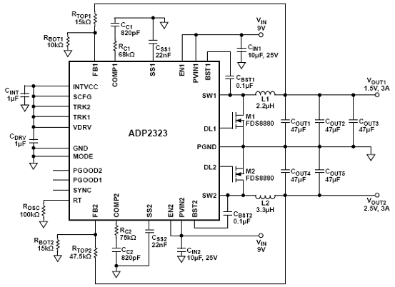
图7.ADP2323 使能PFM模式应用电路图: VIN1 = VIN2 = 9 V, VOUT1 = 1.5 V, IOUT1 = 3 A, VOUT2 = 2.5 V, IOUT2 = 3 A, fSW = 600 kHz 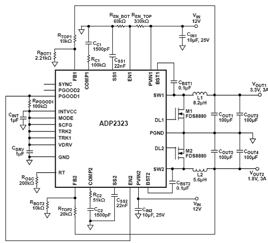
图8.ADP2323可编VIN应用电路图: VIN_RISING = 8.7 V, VIN_FALLING = 6.7 V, 3.3 V Start Up Before 1.8 V, VIN1 = VIN2 = 12 V, VOUT1 = 3.3 V, IOUT1 = 3 A, VOUT2 = 1.8 V, IOUT2 = 3 A, fSW = 300 kHz 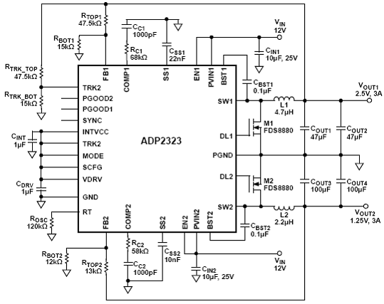
图9.ADP2323通路2跟踪通路1应用电路图:VIN1 = VIN2 = 12 V, VOUT1 = 2.5 V, IOUT1 = 3 A, VOUT2 = 1.25 V, IOUT2 = 3 A, fSW = 500 kHz 详情请见: http://www.analog.com/static/imported-files/data_sheets/ADP2323.pdf |


网友评论