EPC EPC2010 200V 5A氮化镓半桥驱动方案
发布时间:2011-6-6 00:36
发布者:Liming
|
宜普公司(Efficient Power Conversion)的EPC2010是增强型硅基板氮化镓(GaN)功率晶体管,源漏电压200V,漏极电流5A,具有超高的效率,超低的RDS(on)(小于25毫欧姆),超低的QG以及超小的占位面积,其性能优于硅功率MOSFET多倍,主要用在服务器,网路电脑,笔记本电脑,手机,基站,平板显示器以及D-类功率放大器.本文介绍了EPC2010优势和技术指标,以及采用EPC2010的200V半桥栅极驱动器EPC9003开发板方框图,电路图和材料清单和测试框图. Gallium Nitride is grown on Silicon Wafers and processed using standard CMOS equipment leveraging the infrastructure that has been developed over the last 55 years. GaN’s exceptionally high electron mobility and low temperature coefficient allows very low RDS(ON), while its lateral device structure and majority carrier diode provide exceptionally low QG and zero QRR. The end result is a device that can handle tasks where very high switching frequency, and low on-time are beneficial as well as those where on-state losses dominate. EPC2010优势: • Ultra High Efficiency • Ultra Low RDS(on) • Ultra low QG • Ultra small footprint EPC2010主要技术指标: 
EPC2010应用: • High Speed DC-DC conversion • Class D Audio • Hard Switched and High Frequency Circuits 采用EPC2010的200V半桥栅极驱动器EPC9003开发板 EPC has developed the world’s first enhancement mode GaN devices to be offered on the market. Our eGaN FETs provide designers employing any power conversion topology; full bridge, half bridge, buck converter, boost converter, PFC, flyback converter, forward converter, or LLC converter the opportunity to achieve significant performance enhancements compared with silicon power MOSFETs. In order to make EPC’s eGaN FETs easy to use, we developed devices that behave very much like silicon power MOSFETs. User friendly tools make a significant impact in how easy it is to apply a new type of device. EPC’s development boards simplify the evaluation process of our eGaN FETs by including all the critical components and layout for optimal switching performance on a single board that can be easily connected into any existing converter. The EPC9003 development board is a 200 V maximum device voltage, 5 A maximum output current, half bridge with onboard gate drives, featuring the EPC2010 enhancement mode (eGaN®) field effect transistor (FET). The purpose of this development board is to simplify the evaluation process of the EPC2010 eGaN FET by including all the critical components on a single board that can be easily connected into any existing converter. The EPC9003 development board is 2” x 1.5” and contains not only two EPC2010 eGaN FET in a half bridge configuration with gate drivers, but also an on board gate drive supply and bypass capacitors. The board contains all critical components and layout for optimal switching performance. There are also various probe points to facilitate simple waveform measurement and efficiency calculation. 
图1.EPC9003开发板方框图 
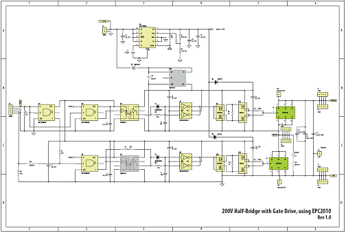
图2.EPC9003开发板电路图 EPC9003开发板材料清单(BOM): 

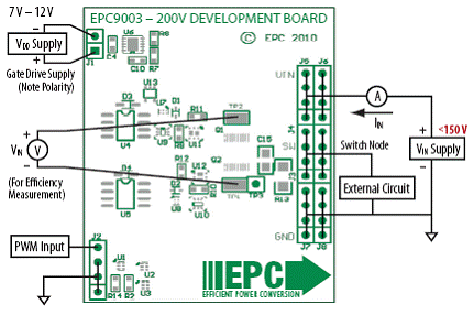
图3.EPC9003开发板连接和测试框图 详情请见: http://epc-co.com/epc/documents/datasheets/EPC2010_datasheet_final.pdf 和 http://epc-co.com/epc/documents/guides/EPC9003_qsg.pdf |


网友评论