ADI AD9739A FMC卡和Xilinx SP605参考设计方案
发布时间:2012-8-2 00:47
发布者:1770309616
|
ADI公司的AD9739A FMC卡是Xilinx SP605, ML605或KC705评估板的子板.两者组成的平台能把MPEG TS流转换成IF或RF信号(单路或多路),并支持大多数数字电视标准(DVB-C,J.83B, DVB-T, ATSC, DVB-S, ...),并可用来评估多种IP核如DVB-C J.83 Annex A/C 调制器,J.83 B有线调制器,DVB-T/H调制器, ATSC调制器,DVB-S调制器等. 主要用在MVD IP核(TS处理,调制,RF上变换).本文介绍了AD9737A/AD9739A产品亮点和主要特性,功能框图以及ADI AD9739A FMC卡+ Xilinx SP605评估平台框图,主要特性和ADI AD9739A FMC评估板电路图. The AD9737A/AD9739A are 11-bit and 14-bit, 2.5 GSPS high performance RF DACs that are capable of synthesizing wideband signals from dc up to 3 GHz. The AD9737A/AD9739A are pin and functionally compatible with the AD9739 with the exception that the AD9737A/AD9739A do not support synchronization or RZ mode, and are specified to operate between 1.6 GSPS and 2.5 GSPS. By elimination of the synchronization circuitry, some nonideal artifacts such as images and discrete clock spurs remain stationary on the AD9737A/AD9739A between power-up cycles, thus allowing for possible system calibration. AC linearity and noise performance remain the same between the AD9739 and the AD9737A/AD9739A. The inclusion of on-chip controllers simplifies system integration. A dual-port, source synchronous, LVDS interface simplifies the digital interface with existing FGPA/ASIC technology. On-chip controllers are used to manage external and internal clock domain variations over temperature to ensure reliable data transfer from the host to the DAC core. A serial peripheral interface (SPI) is used for device configuration as well as readback of status registers. The AD9737A/AD9739A are manufactured on a 0.18 μm CMOS process and operate from 1.8 V and 3.3 V supplies. They are supplied in a 160-ball chip scale ball grid array for reduced package parasitics. AD9737A/AD9739A产品亮点: 1. Ability to synthesize high quality wideband signals with bandwidths of up to 1.25 GHz in the first or second Nyquist zone. 2. A proprietary quad-switch DAC architecture provides exceptional ac linearity performance while enabling mix-mode operation. 3. A dual-port, double data rate, LVDS interface supports the maximum conversion rate of 2500 MSPS. 4. On-chip controllers manage external and internal clock domain skews. 5. Programmable differential current output with an 8.66 mA to 31.66 mA range. AD9737A/AD9739A主要特性: Direct RF synthesis at 2.5 GSPS update rate DC to 1.25 GHz in baseband mode 1.25 GHz to 3.0 GHz in mix-mode Industry leading single/multicarrier IF or RF synthesis Dual-port LVDS data interface Up to 1.25 GSPS operation Source synchronous DDR clocking Pin compatible with the AD9739 Programmable output current: 8.7 mA to 31.7 mA Low power: 1.1 W at 2.5 GSPS AD9737A/AD9739A 应用: Broadband communications systems DOCSIS CMTS systems Military jammers Instrumentation, automatic test equipment Radar, avionics 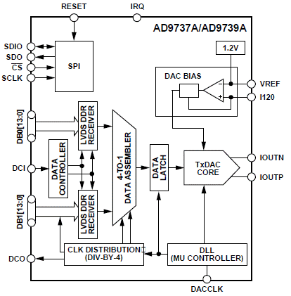
图1.AD9737A/AD9739A功能框图 The AD9739A is a 14-bit, 2.5 GSPS high performance RF DAC capable of synthesizing wideband signals with up to 1.25GHz of bandwidth. This reference design includes a single tone sine generator (DDS) and allows programming the device and monitoring it’s internal status registers. It also programs the ADF4350 clock chip which can generate a 1.6GHz to 2.5GHz clock for the AD9739A from the on-board 25MHz crystal. An alternate clock path using an ADCLK914 is available for driving the clock externally. 
图2.AD9739A FMC评估板外形图 Eval Board w/ an FMC connector for Xilinx based FPGA development The Analog Devices AD9739A FMC card is a daughter board that can be used in addition to Xilinx SP605, ML605 or KC705 evaluation boards. The resulting platform includes all necessary components for the evaluation of most of our IP cores. 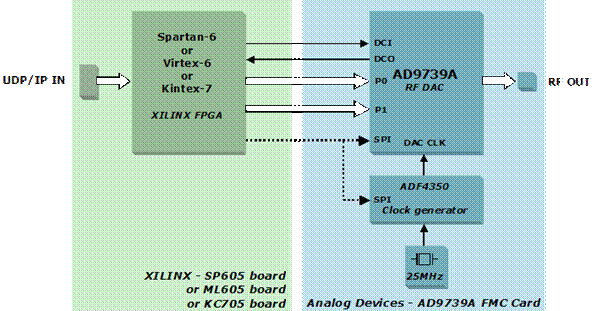
图3.ADI AD9739A FMC卡+ Xilinx SP605评估平台框图 
图4.ADI AD9739A FMC卡+ Xilinx SP605评估平台外形图 ADI AD9739A FMC卡+ Xilinx SP605评估平台主要特性: The evaluation platform converts an MPEG TS stream into an IF or RF signal (single or multi-channel) and supports most of the digital TV standards (DVB-C, J.83B, DVB-T, ATSC, DVB-S, ...). The evaluation platform can be used for the evaluation of our IP cores: DVB-C J.83 Annex A/C modulator J.83 B cable modulator DVB-T/H modulator ATSC modulator DVB-S modulator Digital RF Up Converter DVB Remultiplexer N-to-M Hardware UDP/IP stack RTP transmitter Inputs/Ouputs 1 x UDP/IP input/output for MPEG TS input and IP cores registers configuration (RJ45 connector on Xilinx SP605/ML605/KC705 board) 1 x IF/RF output (SMA connector on Digilent board) Typical applications Evaluation of MVD Cores’ IP cores (TS processing, Modulation, RF Up conversion) 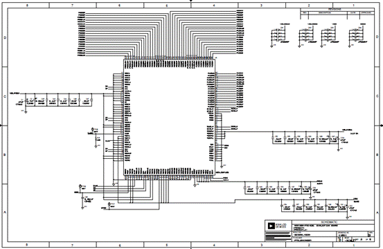
图5.AD9739A FMC评估板电路图(1) 
图6.AD9739A FMC评估板电路图(2) 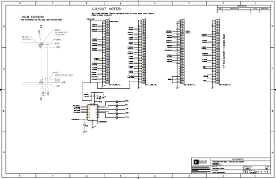
图7.AD9739A FMC评估板电路图(3) 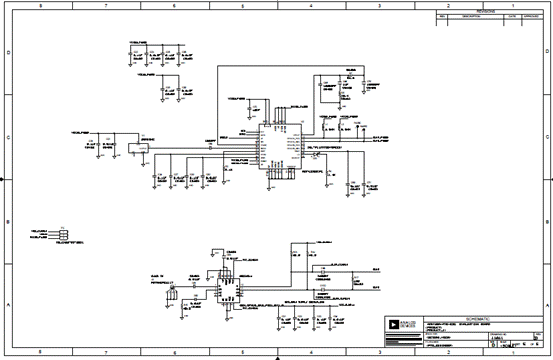
图8.AD9739A FMC评估板电路图(4) 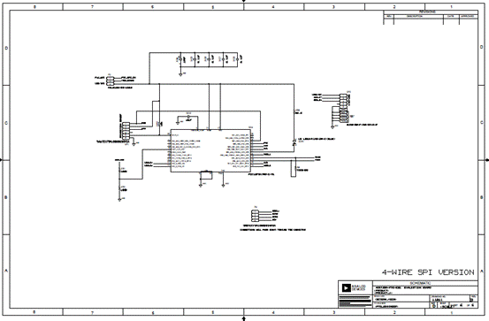
图9.AD9739A FMC评估板电路图(5) 详情请见:  AD9737A_9739A.pdf
(2.65 MB)
和  ad9739a-fmc-ebz_revb_schematic.pdf
(345.06 KB)
来源:网络 |





网友评论