ADI ADuC7060模拟微控制器开发方案
发布时间:2012-8-20 12:34
发布者:1770309616
|
ADI公司的ADuC7060/ADuC7061是低功耗全集成的8 kSPS,24位数据采集系统,在单芯片上集成高性能多通道Σ-Δ型模数转换器(ADC),16位/32位ARM7TDMI® MCU和Flash/EE存储器,包括有4个定时器,高级矢量中断控制器,工作电压2.375 V至2.625 V,工作温度范围为−40℃至+125℃,主要用在工业自动化和过程控制,智能精密检测系统和4 mA至20 mA环路智能传感器。本文介绍了ADuC706x系列主要特性,功能框图,模拟框图以及ADuC7060评估板主要特性,电路图,材料清单和PCB元件布局图. The ADuC706x series are fully integrated, 8 kSPS, 24-bit data acqui-sition systems incorporating high performance multichannel sigma-delta (Σ-Δ) analog-to-digital converters (ADCs), 16-bit/ 32-bit ARM7TDMI®MCU, and Flash/EE memory on a single chip. The ADCs consist of a primary ADC with two differential pairs or four single-ended channels and an auxiliary ADC with up to seven channels. The ADCs operate in single-ended or differential input mode. A single-channel buffered voltage output DAC is available on chip. The DAC output range is programmable to one of four voltage ranges. The devices operate from an on-chip oscillator and a PLL gene-rating an internal high frequency clock up to 10.24 MHz. The microcontroller core is an ARM7TDMI, 16-bit/32-bit RISC machine offering up to 10 MIPS peak performance; 4 kB of SRAM and 32 kB of nonvolatile Flash/EE memory are provided on chip. The ARM7TDMI core views all memory and registers as a single linear array. The ADuC706x contains four timers. Timer1 is a wake-up timer with the ability to bring the part out of power saving mode. Timer2 is configurable as a watchdog timer. A 16-bit PWM with six output channels is also provided. The ADuC706x contains an advanced interrupt controller. The vectored interrupt controller (VIC) allows every interrupt to be assigned a priority level. It also supports nested interrupts to a maximum level of eight per IRQ and FIQ. When IRQ and FIQ interrupt sources are combined, a total of 16 nested interrupt levels is supported. On-chip factory firmware supports in-circuit serial download via the UART serial interface ports and nonintrusive emulation via the JTAG interface. The parts operate from 2.375 V to 2.625 V over an industrial temperature range of −0℃ to +125℃. ADuC706x系列主要特性: Analog input/output Dual (24-bit) ADCs Single-ended and differential inputs Programmable ADC output rate (4 Hz to 8 kHz) Programmable digital filters Built-in system calibration Low power operation mode Primary (24-bit) ADC channel 2 differential pairs or 4 single-ended channels PGA (1 to 512) input stage Selectable input range: ±2.34 mV to ±1.2 V 30 nV rms noise Auxiliary (24-bit) ADC: 4 differential pairs or 7 single-ended channels On-chip precision reference (±10 ppm/°C) Programmable sensor excitation current sources 200 μA to 2 mA current source range Single 14-bit voltage output DAC Microcontroller ARM7TDMI core, 16-/32-bit RISC architecture JTAG port supports code download and debug Multiple clocking options Memory 32 kB (16 kB × 16) Flash/EE memory, including 2 kB kernel 4 kB (1 kB × 32) SRAM Tools In-circuit download, JTAG based debug Low cost, QuickStart™development system Communications interfaces SPI interface (5 Mbps) 4-byte receive and transmit FIFOs UART serial I/O and I2C (master/slave) On-chip peripherals 4× general-purpose (capture) timers including Wake-up timer Watchdog timer Vectored interrupt controller for FIQ and IRQ 8 priority levels for each interrupt type Interrupt on edge or level external pin inputs 16-bit, 6-channel PWM General-purpose inputs/outputs Up to 14 GPIO pins that are fully 3.3 V compliant Power AVDD/DVDD specified for 2.5 V (±5%) Active mode: 2.74 mA (@ 640 kHz, ADC0 active) 10 mA (@ 10.24 MHz, both ADCs active) Packages and temperature range Fully specified for −40℃to +125℃ operation 32-lead LFCSP (5 mm × 5 mm) 48-lead LFCSP and LQFP Derivatives 32-lead LFCSP (ADuC7061) 48-lead LQFP and 48-lead LFCSP (ADuC7060) ADuC706x系列应用: Industrial automation and process control Intelligent, precision sensing systems, 4 mA to 20 mA loop-based smart sensors 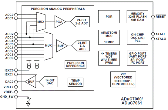
图1.ADuC706x系列功能框图 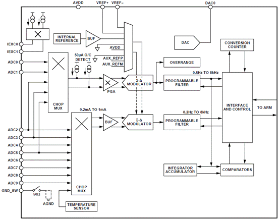
图2.ADuC706x系列模拟框图 ADuC7060评估板 This user guide refers to the ADuC7060 evaluation board. This evaluation board allows evaluation of the ADuC7060 and ADuC7061 parts. The ADuC7060 is the superset of the ADuC706x series, and all features of the ADuC7061 can be evaluated using the ADuC7060. The ADuC7060 contains an ARM7TDMI core, 32 kB of flash, 4 kB of SRAM, dual 24-bit sigma-delta (Σ-Δ) ADCs, and a 12-bit DAC as well as many other features. This evaluation board allows a user to program the ADuC7060 via the JTAG or the UART interfaces. The user may also debug their source code through the JTAG interface. In this user guide, all references to the physical orientation of components on the board are made with respect to a component-side view of the board with the prototype area appearing in the bottom of the board. The board is laid out to minimize coupling between the analog and digital sections of the board. To this end, the ground plane is split with the analog section on the left side and a digital plane on the right side of the board. The regulated 2.5 V power supply is routed directly to the digital section and is filtered before being routed into the analog section of the board. ADuC7060评估板主要特性: 2-layer PCB (4 in. × 5 in. form factor) 9 V power supply regulated to 3.3 V and 2.5 V on board 4-pin UART header to connect to RS-232 interface cable 20-pin standard JTAG connector Demonstration circuit 32.768 kHz watch crystal to drive the PLL clock ADR280 1.2 V external reference chip Reset/download/IRQ0 push buttons Power indicator/general-purpose LEDs Access to all ADC inputs and DAC output from external header; all device ports are brought out to external header pins Surface-mount and through-hole general-purpose prototype area Features true non-intrusive JTAG emulation and an assembly & C-source debugging environment. Hardware Contents.... ADuC7060 Evaluation Board mIDAS-Link JTAG Emulator USB Cable Serial Download Cable International Power Supply 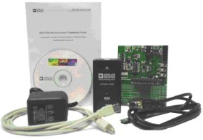
图3.ADuC7060评估板外形图 
图4.ADuC7060评估板电路图(1) 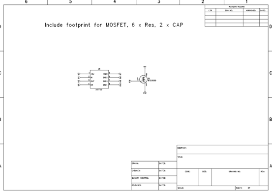
图5.ADuC7060评估板电路图(2) 
图6.ADuC7060评估板电路图(3) ADuC7060评估板材料清单(BOM): 
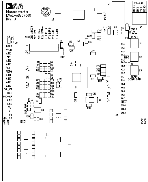
图7.ADuC7060评估板元件布局图 详情请见:  ADuC7060_7061.pdf
(1.56 MB)
 UG-029.pdf
(288.05 KB)
来源:网络 |


网友评论