ADI ADP2441 36V 1A效率94%降压DC电源稳压方案
发布时间:2012-7-13 10:51
发布者:1770309616
|
ADI 公司的ADP2441是36V /1A同步降压DC/DC电源稳压器,负载电流高达1A,输入电压4.5V-36V,输出电压从0.6V到0.9VxVIN,精度±1%,开关频率从300 kHz到1 MHz,效率高达94%,关断电流小于15uA,主要用在POL,分布式电源系统,工业控制电源和DC转换器.本文介绍了ADP2441主要特性,方框图,多种典型应用电路以及ADP2441评估板主要特性,电路图,材料清单和PCB元件布局图. The ADP2441 is a constant frequency, current mode control, synchronous, step-down dc-to-dc regulator that is capable of driving loads up to 1 A with excellent line and load regulation characteristics. The ADP2441 operates with a wide input voltage range of 4.5 V to 36 V, which makes it ideal for regulating power from a wide variety of sources. In addition, the ADP2441 has very low minimum on time (50 ns) and is, therefore, suitable for applications requiring a very high step-down ratio. The output voltage can be adjusted from 0.6 V to 0.9 V × VIN. High efficiency is obtained with integrated low resistance N-channel MOSFETs for both high-side and low-side devices. The switching frequency is adjustable from 300 kHz to 1 MHz with an external resistor. The ADP2441 also has an accurate power-good (PGOOD) open-drain output signal. At light load conditions, the regulator operates in pulse skip mode by skipping pulses and reducing switching losses to improve energy efficiency. In addition, at medium to heavy load conditions, the regulator operates in fixed frequency pulse-width modulation (PWM) mode to reduce electromagnetic interference (EMI). The ADP2441 uses hiccup mode to protect the IC from short circuits or from overcurrent conditions on the output. The external programmable soft start limits inrush current during startup for a wide variety of load capacitances. Other key features include tracking, input undervoltage lockout (UVLO), thermal shutdown (TSD), and precision enable (EN), which can also be used as a logic level shutdown input. The ADP2441 is available in a 3 mm × 3 mm, 12-lead LFCSP package and is rated for a junction temperature range of −0℃ to +125℃. ADP2441主要特性: Wide input voltage range of 4.5 V to 36 V Low minimum on time of 50 ns Maximum load current of 1 A High efficiency of up to 94% Adjustable output down to 0.6 V ±1% output voltage accuracy Adjustable switching frequency of 300 kHz to 1 MHz Pulse skip mode at light load for power saving Precision enable input pin Open-drain power good External soft start with tracking Overcurrent-limit protection Shutdown current of less than 15 μA UVLO and thermal shutdown 12-lead, 3 mm × 3 mm LFCSP package ADP2441应用: Point of load applications Distributed power systems Industrial control supplies Standard rail conversion to 24 V/12 V/5 V/3.3 V 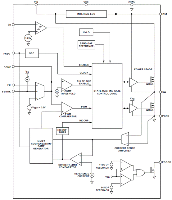
图1.ADP2441方框图 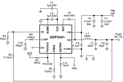
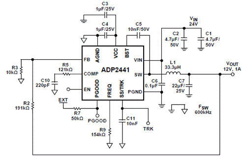
图2.ADP2441典型应用电路图(1): VIN = 24 V ± 10%, VOUT = 5 V, fSW = 700 kHz 图3.ADP2441典型应用电路图(2): VIN = 24 V ± 10%, VOUT = 12 V, fSW = 600 kHz 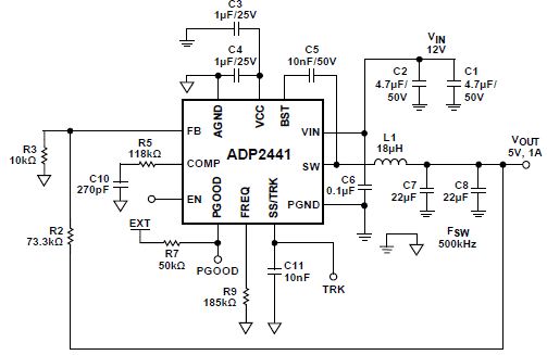
图4.ADP2441典型应用电路图(3): VIN = 12 V ± 10%, VOUT = 5 V, fSW = 500 kHz 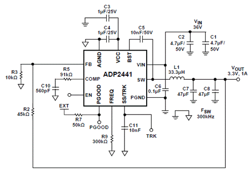
图5.ADP2441典型应用电路图(4): VIN = 36 V ± 10%, VOUT = 3.3 V, fSW = 300 kHz ADP2441评估板 The ADP2441 evaluation board is a complete, dc-to-dc switch-ing regulator design based on the ADP2441, a configurable, 1 A, synchronous step-down, dc-to-dc regulator. The ADP2441 is a synchronous, step-down dc-to-dc switching regulator that uses a current mode pulse-width modulation (PWM) control scheme at medium-to-heavy load currents for high efficiency and smoothly transitions to a pulse skip mode at light loads to conserve power. The power switch and synchronous rectifier are integrated for minimal external part count and high efficiency. The ADP2441 is optimized for operation with small ferrite core inductors and ceramic capacitors to deliver the maximum output power per square millimeter of the PCB board area. The ADP2441-EVALZ is available with 5 V at 1 A output, switching frequency set to 500 kHz. If needed, the ADP2441 evaluation board configuration can be modified by changing the values of the appropriate passive components. Complete specifications for the ADP2441 device can be found in the ADP2441 data sheet, which is available from Analog Devices, Inc., and should be consulted in conjunction with this user guide when using the evaluation board. ADP2441评估板主要特性: Full-featured evaluation board for the ADP2441 Configurable synchronous step down dc-dc switching regulator Operating voltage range of board: VIN = 6 V to 36 V Output voltage is set to 5 V or can be adjusted Maximum load 1 A Switching frequency set to 500 kHz or adjustable switching frequency of 300 kHz to 1 MHz Power saving mode at light load Precision enable input pin Current limit protection Power good output External soft start set to 6 ms or external tracking available Board size: 53 mm × 53 mm 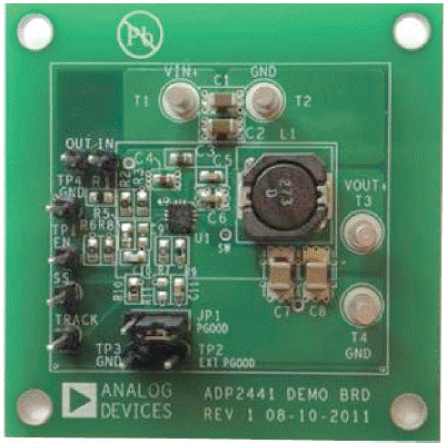
图6.ADP2441评估板外形图 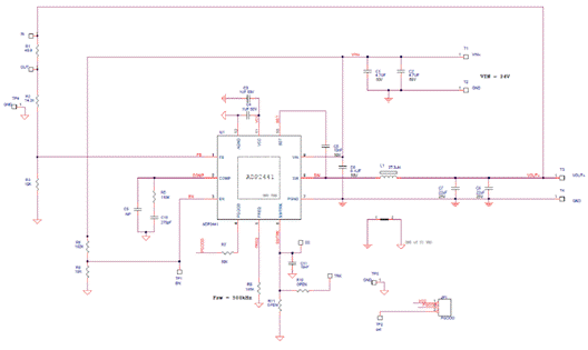
图7.ADP2441评估板电路图 ADP2441评估板材料清单: 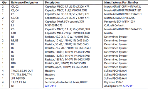
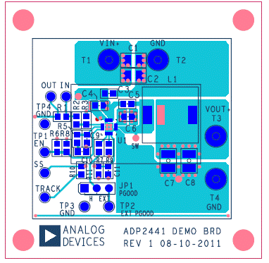
详情请见:  ADP2441.pdf
(1.4 MB)
和  UG-407.pdf
(1.58 MB)
来源:网络 |



网友评论