Freescale i.MX25多媒体应用开发方案
发布时间:2012-5-3 09:27
发布者:1770309616
|
Freescale公司的 i.MX25是用于消费类和工业领域的多媒体应用处理器,采用ARM926EJ-S内核,速度高达具400MHz,具有高性能低功耗特性,支持新兴的工业和通用嵌入市场。i.MX25支持133MHz DDR2存储器,集成了10/100以太网MAC和两个USB PHY,主要用在住宅区网关,工业控制,人机接口(HMI),手持扫描仪和打印机,POS,病人监护仪,图像遥控等。本文介绍了i.MX25多媒体应用处理器主要特性和接口框图,包括SENNA个性板,调试板和i.MX25 CPU引擎板在内的i.MX25 PDK硬件开发系统三件套主要特性,方框图,电路图和材料清单。 The i.MX25 multimedia applications processor has the right mix of high performance, low power, and integration to support the growing needs of the industrial and general embedded markets. At the core of the i.MX25 is Freescale’s fast, proven, power-efficient implementation of the ARM926EJ-S core, with speeds of up to 400 MHz. The i.MX25 includes support for up to 133-MHz DDR2 memory, integrated 10/100 Ethernet MAC, and two on-chip USB PHYs. The device is suitable for a wide range of applications, including the following: • Graphical remote controls • Human Machine Interface (HMI) • Residential and commercial control panels • Residential gateway (smart metering) • Handheld scanners and printers • Electronic point-of-sale terminals • Patient-monitoring devices i.MX25多媒体应用处理器主要特性: • Advanced power management—The heart of the device is a level of power management throughout the IC that enables the multimedia features and peripherals to achieve minimum system power consumption in active and various low-power modes. Power management techniques allow the designer to deliver a feature-rich product that requires levels of power far lower than typical industry expectations. • Multimedia powerhouse—The multimedia performance of the i.MX25 processor is boosted by a 16 KB L1 instruction and data cache system and further enhanced by an LCD controller (with alpha blending), a CMOS image sensor interface, an A/D controller (integrated touchscreen controller), and a programmable Smart DMA (SDMA) controller. • 128 Kbytes on-chip SRAM—The additional 128 Kbyte on-chip SRAM makes the device ideal for eliminating external RAM in applications with small footprint RTOS. The on-chip SRAM allows the designer to enable an ultra low power LCD refresh. • Interface flexibility—The device interface supports connection to all common types of external memories: MobileDDR, DDR, DDR2, NOR Flash, PSRAM, SDRAM and SRAM, NAND Flash, and managed NAND. • Increased security—Because the need for advanced security for tethered and untethered devices continues to increase, the i.MX25 processor delivers hardware-enabled security features that enable secure e-commerce, Digital Rights Management (DRM), information encryption, robust tamper detection, secure boot, and secure software downloads. • On-chip PHY—The device includes an HS USB OTG PHY and FS USB HOST PHY. • Fast Ethernet—For rapid external communication, a Fast Ethernet Controller (FEC) is included. • i.MX25 only supports Little Endian mode. 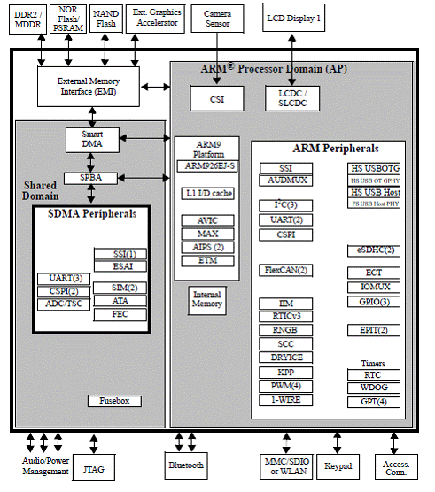
图1。i.MX25简化接口方框图 i.MX25多媒体应用处理器硬件设计文件PDK The i.MX25 3-Stack Platform System helps you to develop multimedia communication applications using the i.MX25 ARM-9 CPU and the MC34704 power management chip. The 3-Stack consists of a CPU Engine board, a Personality board and a Debug board. The system supports application software development, target board debugging, and optional circuit cards. The CPU board can be run in stand-alone mode for code development. A 5’7 LCD display panel is supplied with the 3-Stack. 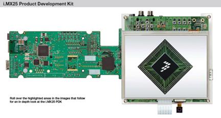
图2。i.MX25 PDK硬件开发系统三件套外形图 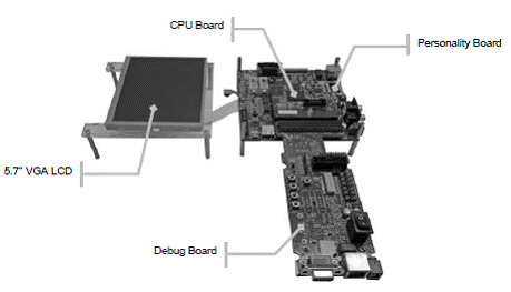
图3。i.MX25 PDK硬件开发系统三件套主要元器件 i.MX25 PDK硬件开发系统主要特性: Near form-factor demonstration modules and working platforms. Solid reference schematics that closely resemble final products to aid customers’ designs. Three-board system, which includes: - CPU board with i.MX25 ARM-9 CPU, MC34704 chip - Personality board with peripheral components and interface connectors - Debug board with two RS232 interfaces, 10/100 Base-T Ethernet connector, and current measure connectors. Utilizes reliable high-density connector to interface between boards. 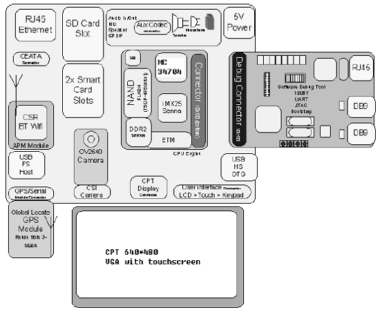
图4。i.MX25 PDK硬件开发系统三件套主板外形图 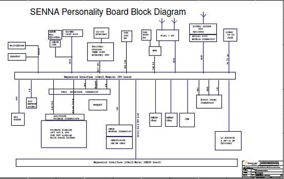
图5。SENNA个性板方框图 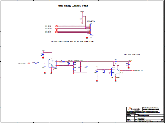
图6。SENNA个性板电路图(1) 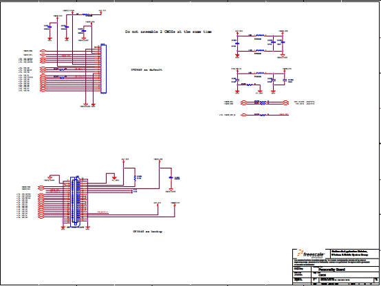
图7。SENNA个性板电路图(2) 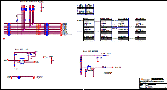
图8。SENNA个性板电路图(3) 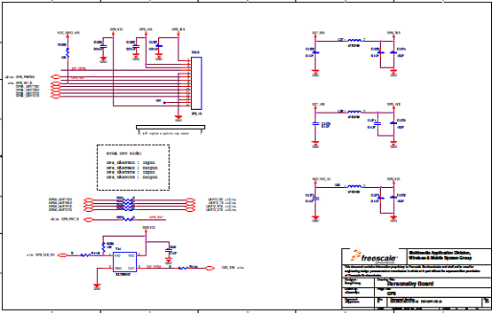
图9。SENNA个性板电路图(4) 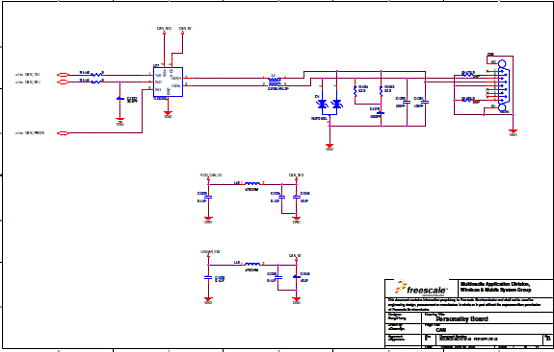
图10。SENNA个性板电路图(5) 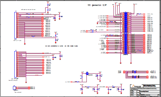
图11。SENNA个性板电路图(6) 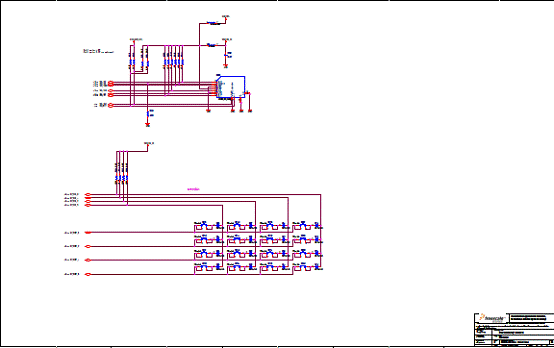
图12。SENNA个性板电路图(7)  图13。SENNA个性板电路图(8) 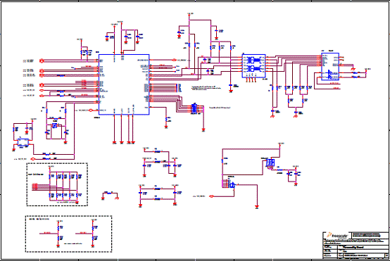
图14。SENNA个性板电路图(9) 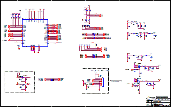
图15。SENNA个性板电路图(10) 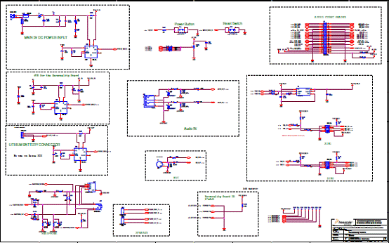
图16。SENNA个性板电路图(11) 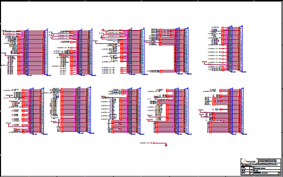
图17。SENNA个性板电路图(12) 
图18。调试板方框图 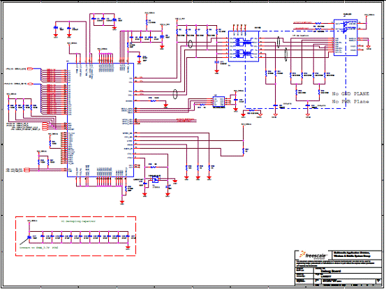
图19。调试板电路图(1) 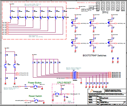
图20。调试板电路图(2) 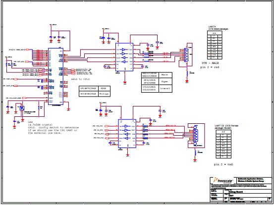
图21。调试板电路图(3) 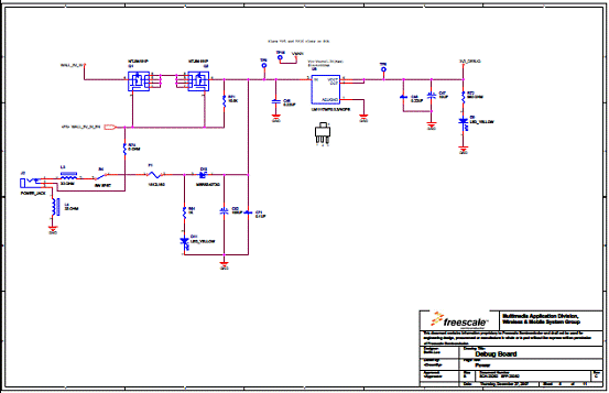
图22。调试板电路图(4) 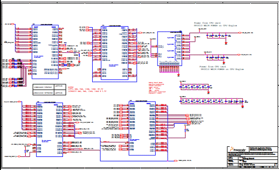
图23。调试板电路图(5) 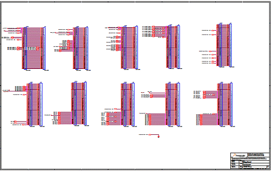
图24。调试板电路图(6) 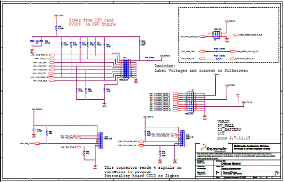
图25。调试板电路图(7) 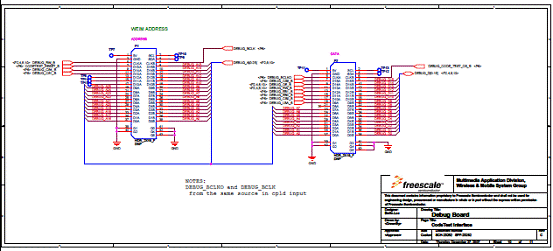
图26。调试板电路图(8) 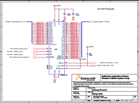
图27。调试板电路图(9) 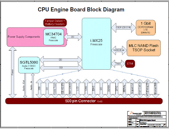
图28。i.MX25 CPU引擎板方框图 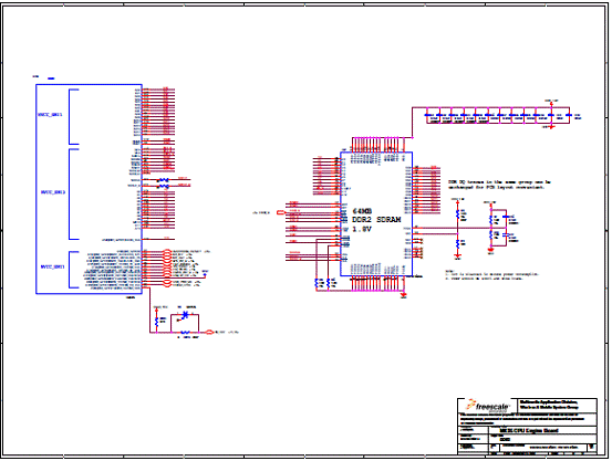
图29。i.MX25 CPU引擎板电路图(1) 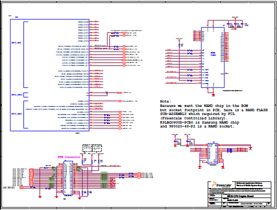
图30。i.MX25 CPU引擎板电路图(2) 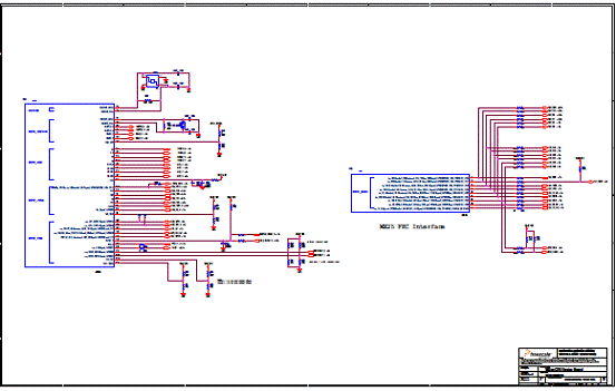
图31。i.MX25 CPU引擎板电路图(3) 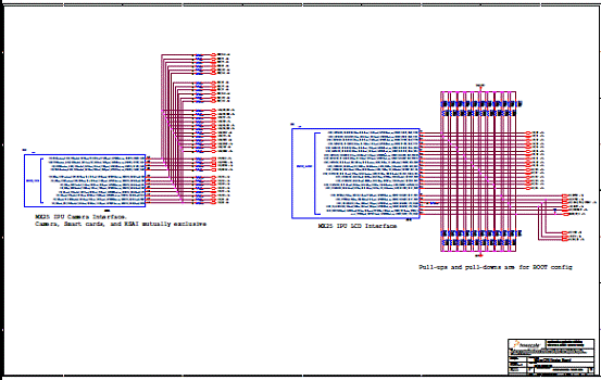
图32。i.MX25 CPU引擎板电路图(4) 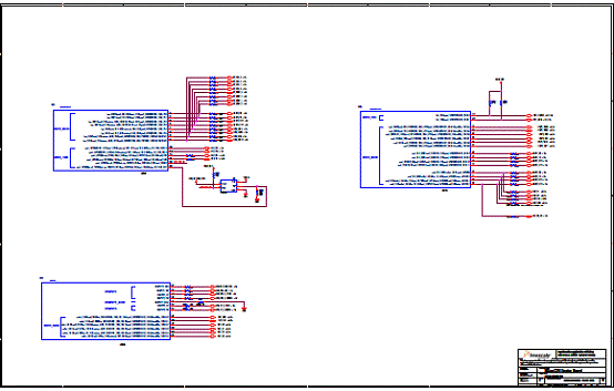
图33。i.MX25 CPU引擎板电路图(5) 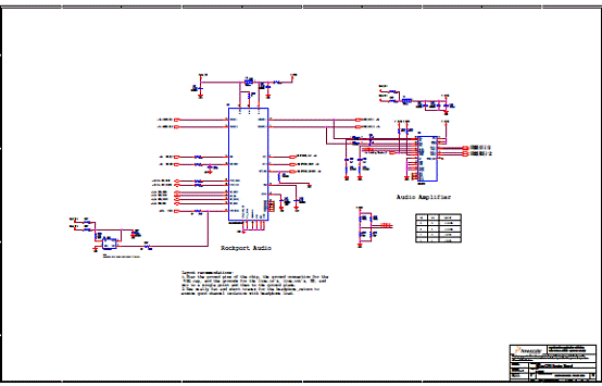
图34。i.MX25 CPU引擎板电路图(6) 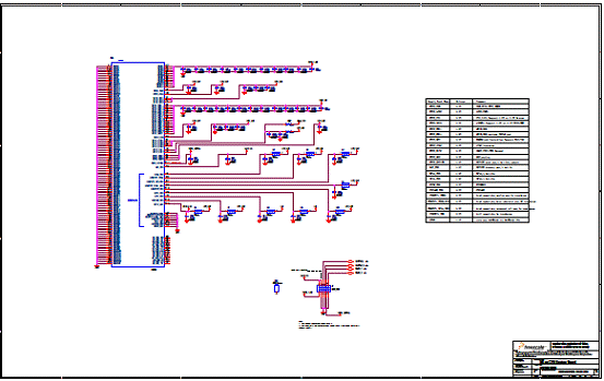
图35。i.MX25 CPU引擎板电路图(7) 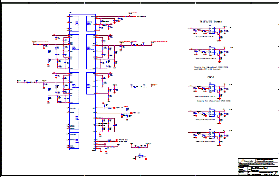
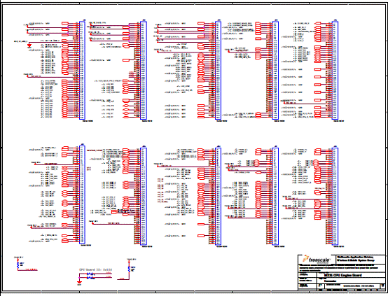
图36。i.MX25 CPU引擎板电路图(8) i.MX25 PDK硬件开发系统材料清单见: 
 i.MX25 PDK硬件开发系统材料清单.rar
(18.01 KB)
详情请见:  pdk10_imx25_Hardware_UG[1].pdf
(2.21 MB)
来源:网络 |


网友评论