Microchip MCP3911用于16位MCU双路模拟前端解决方案
发布时间:2012-4-27 13:39
发布者:1770309616
|
Microchip公司的MCP3911用于16/24位MCU双路模拟前端(AFE),包含两个同时取样的Delta-Sigma ADC,两个PGA,相位延迟补偿区块,低漂移基准电压,调制输出区块,数字失调和增益误差校正寄存器以及高速20MHz SPI兼容串口.每路有 94.5 dB SINAD, -106.5 dBc THD, 111 dB SFDR,2.7-3.6V工作电压,可编数据速率高达125 ksps,主要用在能量和功率测量,汽车,手持仪表,医疗和电源监视以及音/视频识别.本文介绍了MCP3911主要特性,方框图以及用于16位MCU的MCP3911 ADC评估板主要特性, 和PIM MCU连接框图,电路图,材料清单和PCB元件布局图. The MCP3911 is a 2.7V to 3.6V dual channel Analog Front End (AFE) containing two synchronous sampling Delta-Sigma Analog-to-Digital Converters (ADC), two PGAs, phase delay compensation block, low-drift internal voltage reference, modulator output block, digital offset and gain errors calibration registers, and high-speed 20 MHz SPI compatible serial interface. The MCP3911 ADCs are fully configurable with features such as: 16/24-bit resolution, OSR from 32 to 4096, gain from 1x to 32x, independent shutdown and reset, dithering and auto-zeroing. The communication is largely simplified with the one-byte-long commands including various continuous read/write modes that can be accessed by the Direct Memory Access (DMA) of an MCU, and with a separate data ready pin that can be directly connected to an Interrupt Request (IRQ) input of an MCU. The MCP3911 is capable of interfacing a large variety of voltage and current sensors including shunts, current transformers, Rogowski coils and Hall effect sensors. MCP3911主要特性: • Two Synchronous Sampling 16/24-bit Resolution Delta-Sigma A/D Converters • 94.5 dB SINAD, -106.5 dBc Total Harmonic Distortion (THD) (up to 35th harmonic), 111 dB SFDR for Each Channel • 2.7V - 3.6V AVDD, DVDD • Programmable Data Rate up to 125 ksps 4 MHz Maximum Sampling Frequency • Oversampling Ratio up to 4096 • Ultra Low Power Shutdown Mode with <2 μA • -122 dB Crosstalk between the Two Channels • Low Drift 1.2V Internal Voltage Reference: 7 ppm/℃ • Differential Voltage Reference Input Pins • High Gain PGA on Each Channel (up to 32V/V) • Phase Delay Compensation with 1 μs Time Resolution • Separate Modulator Output Pins for Each Channel • Separate Data Ready Pin for Easy Synchronization • Individual 24-bit Digital Offset and Gain Error Correction for Each Channel • High-Speed 20 MHz SPI Interface with Mode 0,0 and 1,1 Compatibility • Continuous Read/Write Modes for Minimum Communication • Low Power Consumption (8.9 mW at 3.3V, 5.6 mW at 3.3V in low-power mode, typical) • Available in Small 20-lead QFN and SSOP Packages, Pin-to-pin Compatible with MCP3901 • Extended Temperature Range: -40℃ to +125℃ MCP3911应用: • Energy Metering and Power Measurement • Automotive • Portable Instrumentation • Medical and Power Monitoring • Audio/Voice Recognition 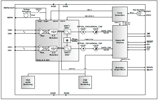
图1.MCP3911方框图 用于16位MCU的MCP3911 ADC评估板 MCP3911 ADC Evaluation Board for 16-Bit MCUs The MCP3911 ADC Evaluation Board for 16-Bit MCUs system provides the opportunity to evaluate the performance of the MCP3911 dual-channel ADC. It also provides a development platform for 16-bit PIC®-based applications, using existing 100-pin PIC microcontroller Plug-in Module (PIM) systems that are compatible with the Explorer 16 and other high pin count PIC®-based demo boards. The system comes with a programmed PIC24FJ256GA110 PIM module that communicates with the Energy Management Utility software for data exchange and ADC setup. MCP3911 ADC评估板亮点: • Dual ADC MCP3911 output display using serial communication to the PC software interface • Simultaneous 55 ksps at OSR32 address loop ALL or 95 dB SINAD at OSR512 performance on MCP3911 • System and ADC performance analysis through graphical PC tools showing noise histogram, frequency domain (FFT), time domain scope plot, and statistical numerical analysis • Robust hardware design with analog grounding and analog/digital separation, allowing low noise evaluation of MCP3911 devices; includes separate power supplies and power planes on a 4-layer board. • PICtail™ Plus connectors for Explorer 16 daughter board compatibility 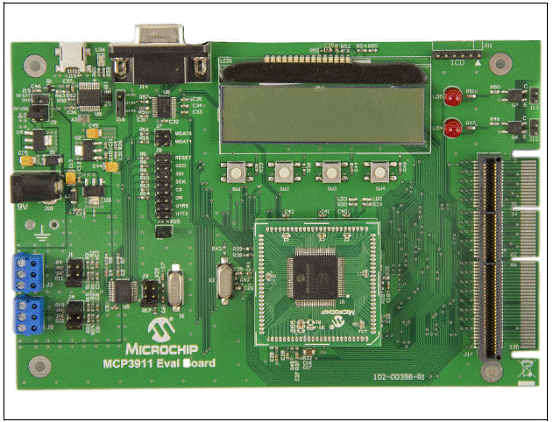
图2.MCP3911评估板外形图 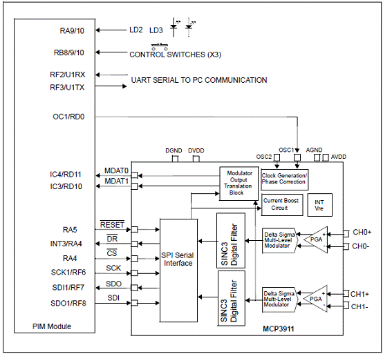
图3.MCP3911和PIM MCU连接框图 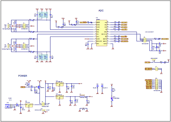
图4.MCP3911评估板电路图:ADC和电源 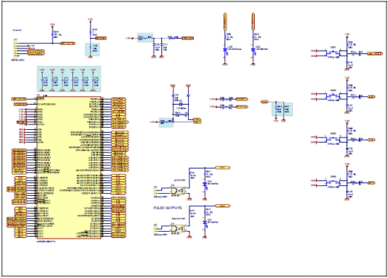
图5.MCP3911评估板电路图:MCU 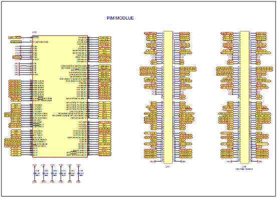
图6.MCP3911评估板电路图  IM模块 IM模块 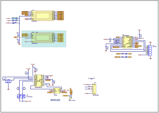
图7.MCP3911评估板电路图  CD和UART CD和UART MCP3911评估板材料清单: 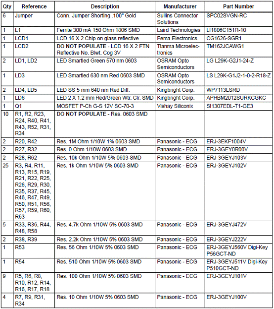
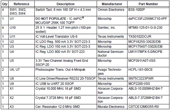
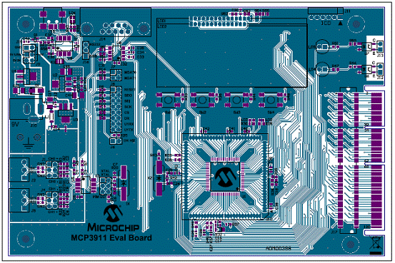
图8.MCP3911评估板PCB布局图:顶层 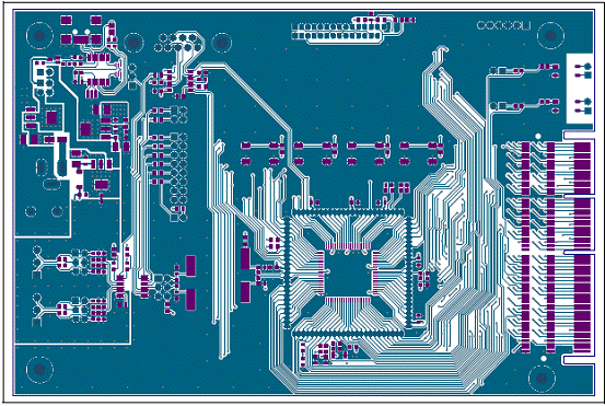
图9.MCP3911评估板PCB布局图:底层 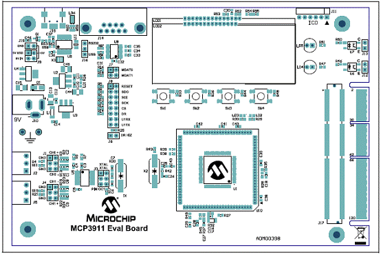
图10.MCP3911评估板元件布局图:顶层 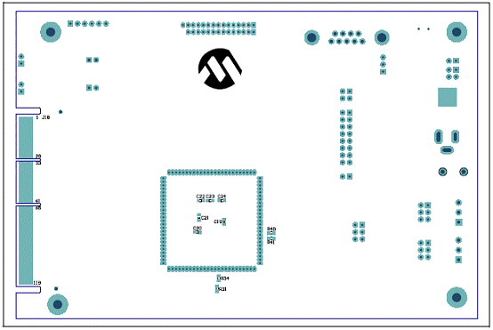
图11.MCP3911评估板元件布局图:底层 详情请见:  22286A.pdf
(1.74 MB)
 52033A.pdf
(1.58 MB)
来源:网络 |



网友评论