Hitex NXP LPC1850 ARM Cortex-M3评估方案
发布时间:2012-3-13 12:05
发布者:1770309616
|
NXP公司的LPC1850/30/20/10是基于ARM Cortex-M3的MCU,工作频率高达180MHz,采用3级流水线和哈佛架构,以及单独的本地指令,数据总线和用于外设的第三条总线,主要用在工业控制,电子仪表,RFID阅读器;消费类电子,白色家电。本文介绍了LPC1850/30/20/10 主要特性和优势,方框图以及Hitex LPC1850评估板主要特性,电路图和元件布局图。 The LPC1850/30/20/10 are ARM Cortex-M3 based microcontrollers for embedded applications. The ARM Cortex-M3 is a next generation core that offers system enhancements such as low power consumption, enhanced debug features, and a high level of support block integration. The LPC1850/30/20/10 operate at CPU frequencies of up to 180 MHz. The ARM Cortex-M3 CPU incorporates a 3-stage pipeline and uses a Harvard architecture with separate local instruction and data buses as well as a third bus for peripherals. The ARM Cortex-M3 CPU also includes an internal prefetch unit that supports speculative branching. The LPC1850/30/20/10 include up to 200 kB of on-chip SRAM, a quad SPI Flash Interface (SPIFI), a State Configurable Timer (SCT) subsystem, two High-speed USB controllers, Ethernet, LCD, an external memory controller, and multiple digital and analog peripherals. LPC1850/30/20/10 主要特性和优势: Processor core ARM Cortex-M3 processor, running at frequencies of up to 180 MHz. ARM Cortex-M3 built-in Memory Protection Unit (MPU) supporting eight regions. ARM Cortex-M3 built-in Nested Vectored Interrupt Controller (NVIC). Non-maskable Interrupt (NMI) input. JTAG and Serial Wire Debug, serial trace, eight breakpoints, and four watch points. Enhanced Trace Module (ETM) and Enhanced Trace Buffer (ETB) support. System tick timer. On-chip memory 200 kB SRAM for code and data use. Multiple SRAM blocks with separate bus access. 64 kB ROM containing boot code and on-chip software drivers. 128 bit One-Time Programmable (OTP) memory for general-purpose use. Clock generation unit Crystal oscillator with an operating range of 1 MHz to 25 MHz. 12 MHz internal RC oscillator trimmed to 1 % accuracy over temperature and voltage. Ultra-low power RTC crystal oscillator. Three PLLs allow CPU operation up to the maximum CPU rate without the need for a high-frequency crystal. The second PLL is dedicated to the High-speed USB, the third PLL can be used as audio PLL. Clock output. Configurable digital peripherals: State Configurable Timer (SCT) subsystem on AHB. Global Input Multiplexer Array (GIMA) allows to cross-connect multiple inputs and outputs to event driven peripherals like timers, SCT, and ADC0/1. Serial interfaces: Quad SPI Flash Interface (SPIFI) with 1-, 2-, or 4-bit data at rates of up to 40 MB per second. 10/100T Ethernet MAC with RMII and MII interfaces and DMA support for high throughput at low CPU load. Support for IEEE 1588 time stamping/advanced time stamping (IEEE 1588-2008 v2). One High-speed USB 2.0 Host/Device/OTG interface with DMA support and on-chip PHY. One High-speed USB 2.0 Host/Device interface with DMA support, on-chip full-speed PHY and ULPI interface to external high-speed PHY. USB interface electrical test software included in ROM USB stack. Four 550 UARTs with DMA support: one UART with full modem interface; one UART with IrDA interface; three USARTs support synchronous mode and a smart card interface conforming to ISO7816 specification. Two C_CAN 2.0B controllers with one channel each. Two SSP controllers with FIFO and multi-protocol support. Both SSPs with DMA support. One Fast-mode Plus I2C-bus interface with monitor mode and with open-drain I/O pins conforming to the full I2C-bus specification. Supports data rates of up to 1 Mbit/s. One standard I2C-bus interface with monitor mode and standard I/O pins. Two I2S interfaces with DMA support, each with one input and one output. Digital peripherals: External Memory Controller (EMC) supporting external SRAM, ROM, NOR flash,and SDRAM devices. LCD controller with DMA support and a programmable display resolution of up to 1024 H 768 V. Supports monochrome and color STN panels and TFT color panels; supports 1/2/4/8 bpp Color Look-Up Table (CLUT) and 16/24-bit direct pixel mapping. SD/MMC card interface. Eight-channel General-Purpose DMA (GPDMA) controller can access all memories on the AHB and all DMA-capable AHB slaves. Up to 164 General-Purpose Input/Output (GPIO) pins with configurable pull-up/pull-down resistors and open-drain modes. GPIO registers are located on the AHB for fast access. GPIO ports have DMA support. Up to 8 GPIO pins can be selected from all GPIO pins as edge and level sensitive interrupt sources. Two GPIO group interrupt modules enable an interrupt based on a programmable pattern of input states of a group of GPIO pins. Four general-purpose timer/counters with capture and match capabilities. One motor control PWM for three-phase motor control. One Quadrature Encoder Interface (QEI). Repetitive Interrupt timer (RI timer). Windowed watchdog timer. Ultra-low power Real-Time Clock (RTC) on separate power domain with 256 bytes of battery powered backup registers. Alarm timer; can be battery powered. Analog peripherals: One 10-bit DAC with DMA support and a data conversion rate of 400 kSamples/s. Two 10-bit ADCs with DMA support and a data conversion rate of 400 kSamples/s. Decryption: Hardware-based AES decryption programmable through an on-chip API. Two 128-bit secure OTP memories for AES key storage and customer use. Unique ID for each device. Power: Single 3.3 V (2.2 V to 3.6 V) power supply with on-chip internal voltage regulator for the core supply and the RTC power domain. RTC power domain can be powered separately by a 3 V battery supply. Four reduced power modes: Sleep, Deep-sleep, Power-down, and Deep power-down. Processor wake-up from Sleep mode via wake-up interrupts from various peripherals. Wake-up from Deep-sleep, Power-down, and Deep power-down modes via external interrupts and interrupts generated by battery powered blocks in the RTC power domain. Brownout detect with four separate thresholds for interrupt and forced reset. Power-On Reset (POR). Available as 208-pin, 144-pin, and 100-pin LQFP packages and as 256-pin, 180-pin, and 100-pin BGA packages. LPC1850/30/20/10 应用: Industrial Consumer White goods RFID readers e-Metering 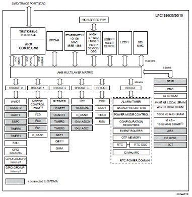
图1。LPC1850/30/20/10方框图 Hitex LPC1850评估板 The Hitex LPC1850 Eval board allows you to quickly and easily evaluate the LPC1800 family of microcontrollers. The microcontroller, board, and the accompanying features make it a great starting point for your next Cortex-M3 project. Populated with the LPC1850 to demonstrate LPC1800 features, the LPC1850 offers industry leading performance, large internal memories and advanced peripherals. The board is USB-powered, but can also be driven by external power supply or via power-over-Ethernet. It is equipped with 65MB SDRAM, 32MB parallel flash and 512kB SRAM and a serial EEPROM. For debugging a JTAG as well as a 20-pin Cortex debug connector with ETM is available. All channels (USB1 and USB2) as well as Ethernet are provided by Phy. This makes USB device, USB host and OTG available as well as UART and CAN. Hitex LPC1850评估板主要特性: The evaluation board has the following features: - CPU: LPC1850 (ARM Cortex-M3) - Power-over-Ethernet - Ready for energy consumption analysis with PowerScale of the complete board, the CPU-core and other peripherals - SDRAM, SRAM, parallel flash, NAND flash, qSPI flash - Temperature sensor, SD card, media-connector - CAN, UART, Ethernet, USB (Host, Device, OTG) - Debug with standard ARM JTAG and JTAG + Trace connector - Ready for Jennic ZigBee module - Small onboard display and NXP standard display / LCD interface - Touch buttons and LEDs - Wrap field for user circuits - Audio IN and OUT, microphone IN, headphones OUT and a D-Class amplifier - Ready for 4x ADC1415 analog-to-digital converters with user filtering option 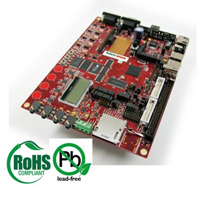
图2。Hitex LPC1850评估板外形图 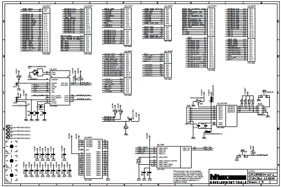
图3。Hitex LPC1850评估板电路图(1) 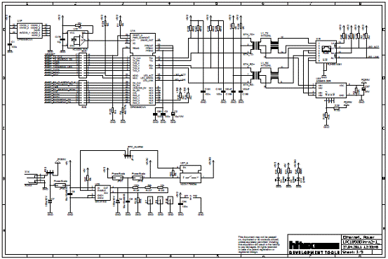
图4。Hitex LPC1850评估板电路图(2) 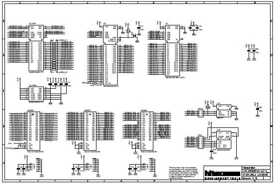
图5。Hitex LPC1850评估板电路图(3) 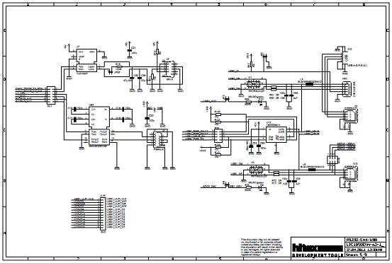
图6。Hitex LPC1850评估板电路图(4) 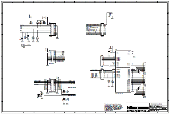
图7。Hitex LPC1850评估板电路图(5) 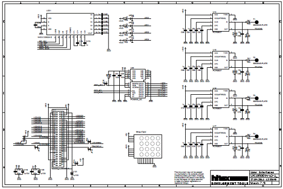
图8。Hitex LPC1850评估板电路图(6) 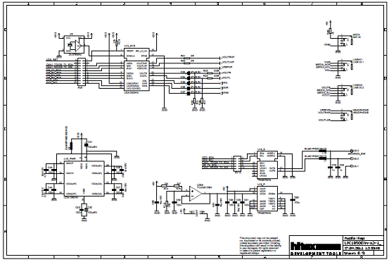
图9。Hitex LPC1850评估板电路图(7) 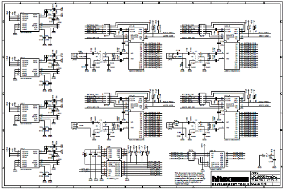
图10。Hitex LPC1850评估板电路图(8) 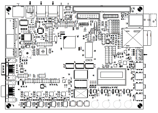
图11。Hitex LPC1850评估板元件布局图 详情请见:  LPC1850_30_20_10[1].pdf
(2.72 MB)
 Hitex_LPC1850_Eval_Board_Schematics[1].pdf
(245.67 KB)
来源:网络 |




网友评论