AKM AK7782ЫЋТЗвєЦЕаХКХДІРэНтОіЗНАИ
ЗЂВМЪБМфЃК2012-3-13 11:39
ЗЂВМепЃК1770309616
|
AKM ЙЋЫОЕФAK7782ЪЧМЏГЩ24ЮЛ5ТЗADCКЭSRCЕФЫЋТЗвєЦЕаХКХДІРэЦї(DSP),ЭЌЪБЛЙМЏГЩСЫ8:2СЂЬхЩљЪфШыбЁдёЦї,ШЁбљЫйТЪзЊЛЛЦї,ЫйТЪИпДя96kHz,ADCШЁбљЦЕТЪДг7.35kHz ЕН96kHz.БОЮФНщЩмСЫAK7782жївЊЬиад,ЗНПђЭМ,DSPЗНПђЭМ,AK7782ЦРЙРАхAKD7782-AжївЊЙІФм,ЗНПђЭМ,ЕчТЗЭМвдМАдЊМўВМОжЭМ. The AK7782 is an audio digital signal processor with integrated 24bit 5ch ADCs, an 8:2 stereo input selector and sample rate converters that support 2ch inputs and the frequency up to 96kHz. The ADC supports wide range of sampling frequency from 7.35kHz to 96kHz. Two integrated audio DSPs have high performance processing speed of 2560step/fs (at 48kHz sampling), and two 6k-word delay RAMs allow surround processing, time alignment adjusting and FIR filtering. As the AK7782 is a RAM based DSP, it is programmable for various user requirements. It is housed in a 100pin LQFP package. AK7782жївЊЬиад: [DSP1/DSP2] Ёѕ Word Length: 28-bits Ёѕ Instruction Cycle Time: 8.1ns (2560fs, fs=48kHz) Ёѕ Processing Step: 2560 steps (max) /fs= 48kHz, 44.1kHz (Normal Speed) 15360 steps (max) /fs= 8kHz, 7.35kHz 1280 steps (max) fs= 96kHz, 88.2kHz (Double Speed) Ёѕ Multiplier: 24 x 16 Ёњ 40-bits (double precision available) Ёѕ Divider: 24 ЁТ 24 Ёњ 24-bits (floating point normalization function) Ёѕ ALU: 44-bit arithmetic operation (with 4-bit overflow margin) 24-bit arithmetic and logic operation Ёѕ Data Shift: Right shift after multiplication 1, 2, 4, 5, 8, 14, 15-bits Right shift BUS 1, 2, 3, 4, 8, 14, 15-bits Left shift after multiplication 1, 2, 3, 4, 8, 15-bits Left shift BUS 1, 2, 3, 4, 6, 8, 15-bits Indirect shifting function Ёѕ Program RAM (PRAM): 2048word x 36-bits Ёѕ Coefficient RAM (CRAM): 2048word x 16-bits Ёѕ Data RAM (DRAM): 2048word x 28-bits Ёѕ Offset Register (OFREG): 64word x 13-bits Ёѕ Delay RAM (DLRAM): 168kbit (four types) Ёё 6kword 28-bits Ёё 4kword 28-bits + 4kword 14-bits Ёё 3kword 28-bits + 6kword 14-bits Ёё 3kword 28-bits + 3kword 28-bits (Linear) Ёѕ Register: 44-bits x 4 (ACC) [for ALU] 28-bits x 12 (TMP) [DBUS connection] 28-bits x 6 steps stack (PTMP) [DBUS connection] [Stereo ADC, Common for ADC1 and ADC2] Ёѕ 24-bit 2ch x 2 Ёѕ S/(N+D): 90dB (fs=48kHz) Ёѕ D-range: 96dBA (fs=48kHz) Ёѕ S/N: 96dBA (fs=48kHz) Ёѕ 8ch bidirectional analog input selector Ёѕ High-pass filter (HPF) for DC offset cancellation Ёѕ fs=7.35kHz ~ 96kHz[Mono ADC] Ёѕ 24bit 1ch Ёѕ S/(N+D) 88dB (fs=48kHz) Ёѕ D-range 95dBA (fs=48kHz) Ёѕ S/N 95dBA (fs=48kHz) Ёѕ High-pass filter (HPF) for DC offset cancellation Ёѕ fs=7.35kHz ~ 96kHz Ёѕ Digital volume control[DSP1/DSP2 In/Output Digital Interface] Ёѕ Serial Data Input: 14ch (including ADC block) Ёѕ Serial Data Output: 16ch (each DSP outputs are 14ch) Ёѕ Microcomputer Interface: 1ch In/Out or I2C-bus[SRC, Common for SRC1 and SRC2] Ёѕ 2ch x 2 Ёѕ fs=7.35kHz ~ 96kHz [General] Ёѕ PLL Ёѕ 3.3VЁР0.3V, 1.8V ЁР0.1V Ёѕ Operational Temperature: -40Ёц ~ 85Ёц Ёѕ 100pin LQFP 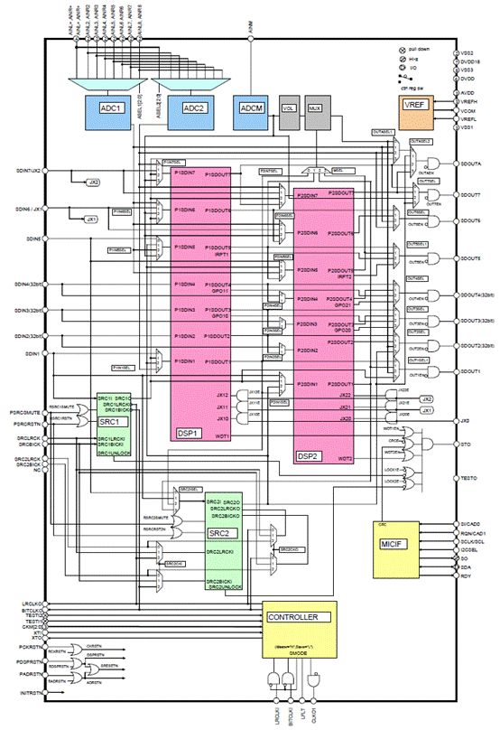
ЭМ1.AK7782ЗНПђ 
ЭМ2.AK7782 DSPЗНПђЭМ ( DSP1 КЭDSP2) AK7782ЦРЙРАхAKD7782-A The AKD7782-A is an evaluation board for AK7782, which is a highly integrated audio processor including 5ch 24bit ADC, 4ch SRC and two audio DSP cores. This board is composed of a main board and a sub board. It is possible to control the setting of board via USB port. RCA connectors are used for the input and output of analog signal. This board also has digital interface and can achieve the interface with digital audio system via optical connector. ЦРЙРАхAKD7782-AЙІФм: Read/Write access to PRAM, CRAM, OFREG and control registers of AK7782 Compatible with 2 types of digital audio interface - Optical input (x1) / Optical output (x1) - 10pin header for interface with external data source (x2) ADC1/ADC2 18ch input, ADCM 1ch input, DAC 8ch output(Note: There is no DAC within AK7782. 8ch DAC AK4359 is equipped.) USB port for board control 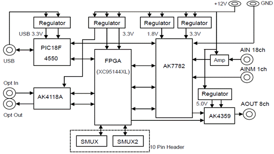
ЭМ3.AKD7782-A ЗНПђЭМ 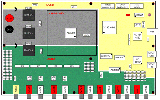
ЭМ4.AKD7782-A ЦРЙРАхЗНПђЭМ 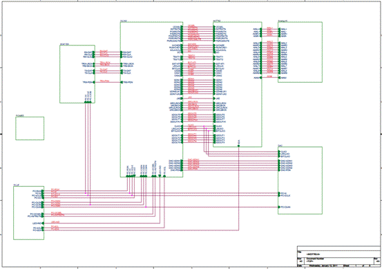
ЭМ5.AKD7782-A ЦРЙРАхЕчТЗЭМ(1) 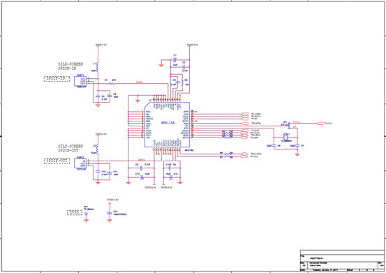
ЭМ6.AKD7782-A ЦРЙРАхЕчТЗЭМ(2) 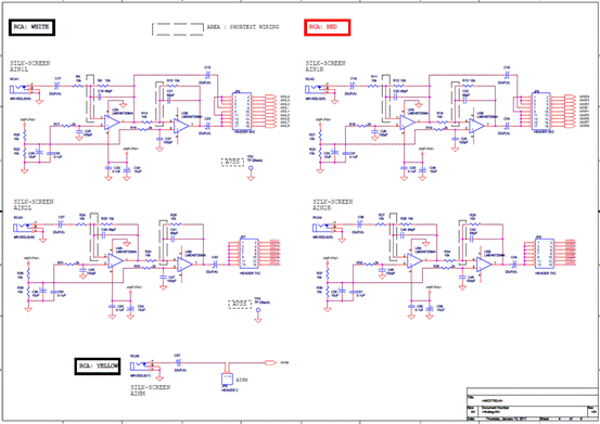
ЭМ7.AKD7782-A ЦРЙРАхЕчТЗЭМ(3) 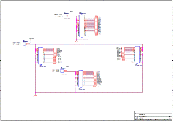
ЭМ8.AKD7782-A ЦРЙРАхЕчТЗЭМ(4) 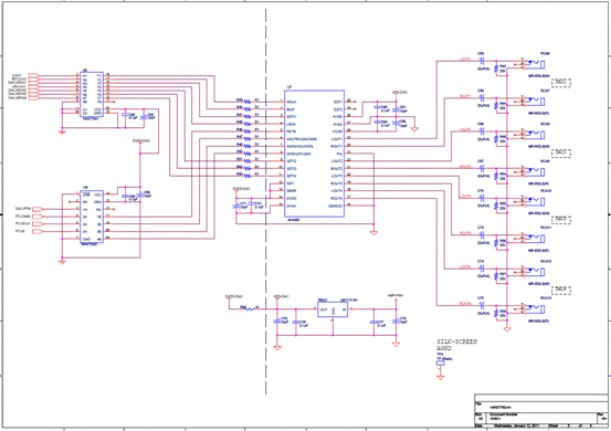
ЭМ9.AKD7782-A ЦРЙРАхЕчТЗЭМ(5) 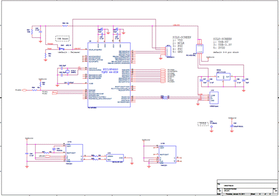
ЭМ10.AKD7782-A ЦРЙРАхЕчТЗЭМ(6) 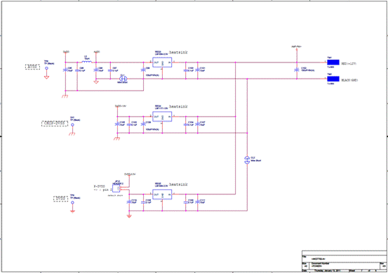
ЭМ11.AKD7782-A ЦРЙРАхЕчТЗЭМ(7) 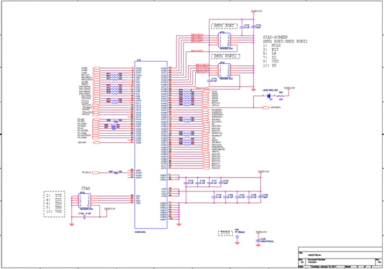
ЭМ12.AKD7782-A ЦРЙРАхЕчТЗЭМ(8) 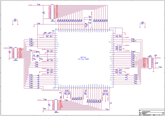
ЭМ13.AKD7782-A ЦРЙРАхЕчТЗЭМ(9) 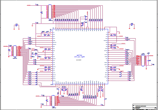
ЭМ14.AKD7782-A ЦРЙРАхЕчТЗЭМ(10) 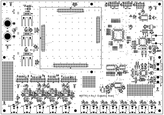
ЭМ15.AKD7782-A ЦРЙРАхдЊМўВМОжЭМ ЯъЧщЧыМћ:  ak7782_f00_pbe[1].pdf
(384.08 KB)
 akd7782-a0-00e[1].pdf
(2.41 MB)
РДдДЃКЭјТч |


ЭјгбЦРТл