Freescale PXS20三相太阳能逆变器解决方案
发布时间:2012-2-17 12:37
发布者:1770309616
|
Freescale公司的PXS20是32位双核双发射的Power Architecture微控制器,满足安全标准IEC61511和IEC61508 (SIL3),能降低设计复杂性和减少所用元件.PXS20采用高性能的e200z4d双核,核频率高达120MHz,双发射级流水线核,可变长度编码(VLE),集成了存储器管理单元(MMU)和信号处理引擎,带误差检测代码的4KB指令缓存,主要用在消费类电子,工业控制,太阳能逆变器,机器人和马达控制等.本文介绍了PXS20主要特性,方框图,以及采用PXS20控制的太阳能三相逆变器基本架构,1kW, 3kW,10kW和大于10kW以及微逆变器的太阳能三相逆变器解决方案架构图. The PXS20 family of 32-bit Power Architecture® microcontrollers is designed to specifically address the requirements of the safety standards IEC61511 and IEC61508 (SIL3). It reduces design complexity and component count by putting key functional safety features on a single chip with a dual-core, dual-issue architecture, which can be statically switched between lockstep mode (redundant processing and calculations) to decoupled parallel mode (independent core operation). The PXS20 microcontrollers are SafeAssure solutions. The PXS20 series microcontrollers are system-on-chip devices that are built on Power Architecture technology and contain enhancements that improve the architecture’s fit in embedded applications, include additional instruction support for digital signal processing (DSP) and integrate technologies such as an enhanced time processor unit, enhanced queued analog-to-digital converter, Controller Area Network, and an enhanced modular input-output system. The PXS20 family of 32-bit microcontrollers is the latest achievement in integrated safety controllers. The advanced and cost-efficient host processor core of the PXS20 family complies with the Power Architecture embedded category. It operates at speeds as high as 120 MHz and offers high-performance processing optimized for low power consumption. It capitalizes on the available development infrastructure of current Power Architecture devices and is supported with software drivers, operating systems and configuration code to assist with users’ implementations. PXS20主要特性: • High-performance e200z4d dual core – 32-bit Power Architecture® technology CPU – Core frequency as high as 120 MHz – Dual issue five-stage pipeline core – Variable Length Encoding (VLE) – Memory Management Unit (MMU) – 4 KB instruction cache with error detection code – Signal processing engine (SPE) • Memory available – 1 MB flash memory with ECC – 128 KB on-chip SRAM with ECC – Built-in RWW capabilities for EEPROM emulation • SIL3/ASILD innovative safety concept: LockStep mode and Fail-safe protection Sphere of replication (SoR) for key components (such as CPU core, eDMA, crossbar switch) – Fault collection and control unit (FCCU) – Redundancy control and checker unit (RCCU) on outputs of the SoR connected to FCCU – Boot-time Built-In Self-Test for Memory (MBIST) and Logic (LBIST) triggered by hardware – Boot-time Built-In Self-Test for ADC and flash memory triggered by software – Replicated safety enhanced watchdog – Replicated junction temperature sensor – Non-maskable interrupt (NMI) – 16-region memory protection unit (MPU) – Clock monitoring units (CMU) – Power management unit (PMU) – Cyclic redundancy check (CRC) unit • Decoupled Parallel mode for high-performance use of replicated cores • Nexus Class 3+ interface • Interrupts – Replicated 16-priority controller – Replicated 16-channel eDMA controller • GPIOs individually programmable as input, output or special function • Three 6-channel general-purpose eTimer units • 2 FlexPWM units – Four 16-bit channels per module • Communications interfaces – 2 LINFlexD channels – 3 DSPI channels with automatic chip select generation – 2 FlexCAN interfaces (2.0B Active) with 32 message objects FlexRay module (V2.1 Rev. A) with 2 channels, 64 message buffers and data rates up to 10 Mbit/s • Two 12-bit analog-to-digital converters (ADCs) – 16 input channels – Programmable cross triggering unit (CTU) to synchronize ADCs conversion with timer and PWM • Sine wave generator (D/A with low pass filter) • On-chip CAN/UART bootstrap loader • Single 3.0 V to 3.6 V voltage supply • Ambient temperature range –40℃ to 125℃ • Junction temperature range –40℃ to 150℃ PXS20目标应用: Consumer: Boiler Heating Control Industrial Programmable Logic Control (PLC) Input-Output Control (I/O Control) Off-Grid Solar Power Inverters Commercial Solar Power Inverters Residential Solar Power Inverters Unmanned Vehicles (Ground, Air, Water) Motion Control Process Control Robot Manipulator Robotic Arm Medical/Healthcare Anesthesia Unit Monitor Ventilators and Respirators Motor Control Stepper Motor 
图1. PXS20方框图 采用PXS20控制的太阳能三相逆变器 Solar Panel 3-Phase Inverter Controlled by the PXS20 Today, the demand for green energy is very strong. One possible option for meeting this demand is to convert solar energy into electrical energy. This process is supported by the photovoltaic (PV) solar panel, which produces various DC output voltages and output power. In the conversion from DC to AC power, dedicated inverters maintain the right working point for the solar panel to maximize its use of solar energy. Freescale Semiconductor’s processors built on Power Architecture® technology are well suited for the control of such inverters. Freescale offers a broad portfolio of PX microcontrollers built on Power Architecture technology for power management and motor control applications. The target portfolio for these devices includes consumer, industrial, and other markets. One microcontroller from the PX Series of Power Architecture devices can control the whole 3-phase inverter in various configurations and output power. 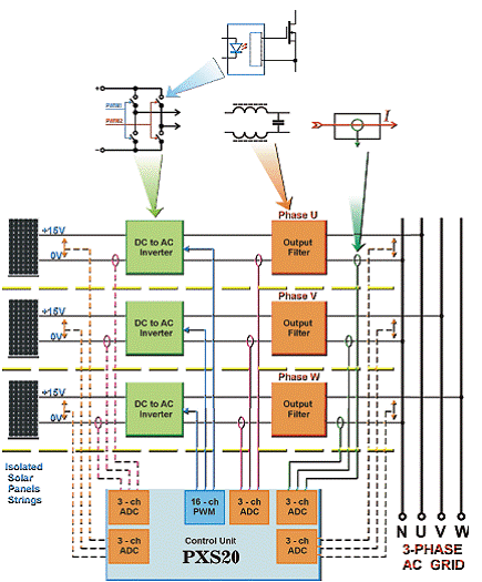
图2.太阳能三相逆变器基本架构图 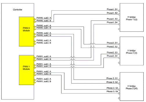
图3.采用H桥拓扑的太阳能三相逆变器的PWM连接框图 The demonstrator uses a standard PXS20 controller board and a 3-phase inverter analog board that can support an H-bridge or H5 topology. The input of each phase is represented by the isolated 15V DC power supplies (replacing the solar panels in this demonstrator). The control and measurement circuitry can be powered by the separated DC power source, or by one of the phase power sources. 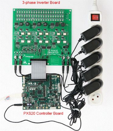
图4.太阳能三相逆变器演示板外形图 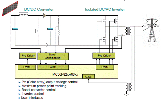
图5.小于1kW的太阳能三相逆变器解决方案 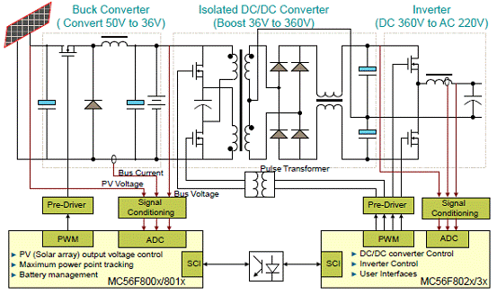
图6.小于3kW的太阳能三相逆变器解决方案 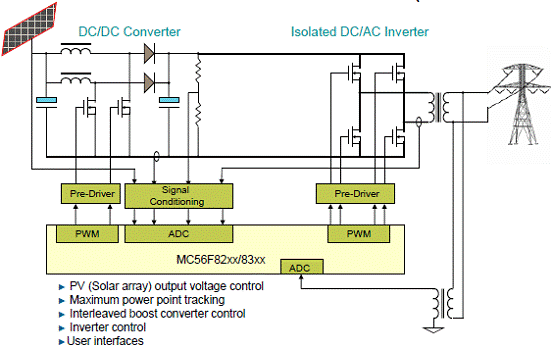
图7.小于10kW的太阳能三相逆变器解决方案 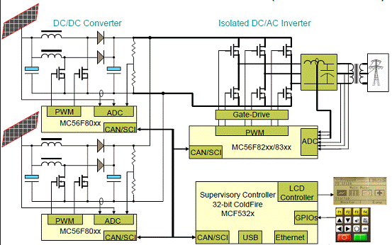
图8.大于10kW的太阳能三相逆变器解决方案 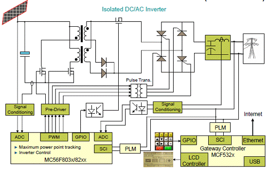
图9.太阳能微逆变器解决方案 详情请见:  PXS20[1].pdf
(661.1 KB)
 AN4437[1].pdf
(3.44 MB)
来源:网络 |


网友评论