ADI ADuC702x脉搏血氧仪解决方案
发布时间:2011-12-28 08:45
发布者:1046235000
|
脉搏血氧仪以非介入方式测量血液中的含氧量,包括发射路径,接收路径,显示和背光,数据接口以及音频报警。发射路径包括红光LED,红外光LED和用于驱动LED的DAC。接收路径包括光电二极管传感器,信号调理,模数转换器和处理器。ADI的脉搏血氧仪解决方案采用ADuC7024精密模拟微控制器,具有多达16路的12位1MSPS的ADC和采用ARM7TDMI核16位/32位RISC架构的MCU.本文介绍了ADuC7019/20/21/22/24/25/26/27/28/29主要特性和功能框图, ADuC7024评估板主要特性, 电路图和材料清单,以及ADI脉搏血氧仪功能框图及其主要元件表, 脉搏血氧仪演示系统框图和所用的主要产品表. The ADuC7019/20/21/22/24/25/26/27/28/29 are fully integrated, 1 MSPS, 12-bit data acquisition systems incorporating high performance multichannel ADCs, 16-bit/32-bit MCUs, and Flash®/EE memory on a single chip. The ADC consists of up to 12 single-ended inputs. An additional four inputs are available but are multiplexed with the four DAC output pins. The four DAC outputs are available only on certain models (ADuC7020, ADuC7026, ADuC7028, and ADuC7029). However, in many cases where the DAC outputs are not present, these pins can still be used as additional ADC inputs, giving a maximum of 16 ADC input channels. The ADC can operate in single-ended or differential input mode. The ADC input voltage is 0 V to VREF. A low drift band gap reference, temperature sensor, and voltage comparator complete the ADC peripheral set. Depending on the part model, up to four buffered voltage output DACs are available on-chip. The DAC output range is programmable to one of three voltage ranges. The devices operate from an on-chip oscillator and a PLL generating an internal high frequency clock of 41.78 MHz (UCLK). This clock is routed through a programmable clock divider from which the MCU core clock operating frequency is generated. The microcontroller core is an ARM7TDMI®, 16-bit/32-bit RISC machine, which offers up to 41 MIPS peak performance. Eight kilobytes of SRAM and 62 kilobytes of nonvolatile Flash/EE memory are provided on-chip. The ARM7TDMI core views all memory and registers as a single linear array. On-chip factory firmware supports in-circuit serial download via the UART or I2C serial interface port; nonintrusive emulation is also supported via the JTAG interface. These features are incorporated into a low cost QuickStart™ development system supporting this MicroConverter® family. The parts operate from 2.7 V to 3.6 V and are specified over an industrial temperature range of −40℃ to +125℃. When operating at 41.78 MHz, the power dissipation is typically 120 mW. The ADuC7019/20/21/22/24/25/26/27/28/29 are available in a variety of memory models and packages (see Ordering Guide). ADuC7019/20/21/22/24/25/26/27/28/29主要特性: Analog I/O Multichannel, 12-bit, 1 MSPS ADC Up to 16 ADC channels1 Fully differential and single-ended modes 0 V to VREF analog input range 12-bit voltage output DACs Up to 4 DAC outputs available1 On-chip voltage reference On-chip temperature sensor (±3°C) Voltage comparator Microcontroller ARM7TDMI core, 16-bit/32-bit RISC architecture JTAG port supports code download and debug Clocking options Trimmed on-chip oscillator (±3%) External watch crystal External clock source up to 44 MHz 41.78 MHz PLL with programmable divider Memory 62 kB Flash/EE memory, 8 kB SRAM In-circuit download, JTAG-based debug Software-triggered in-circuit reprogrammability On-chip peripherals UART, 2× I2C® and SPI serial I/O Up to 40-pin GPIO port1 4× general-purpose timers Wake-up and watchdog timers (WDT) Power supply monitor 3-phase, 16-bit PWM generator1 Programmable logic array (PLA) External memory interface, up to 512 kB1 Power Specified for 3 V operation Active mode: 11 mA @ 5 MHz, 40 mA @ 41.78 MHz Packages and temperature range From 40-lead 6 mm × 6 mm LFCSP to 80-lead LQFP1 Fully specified for –40℃ to +125℃ operation Tools Low cost QuickStart™ development system Full third-party support ADuC7019/20/21/22/24/25/26/27/28/29应用: Industrial control and automation systems Smart sensors, precision instrumentation Base station systems, optical networking 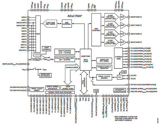
图1.ADuC7026方框图 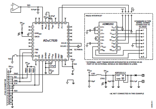
图2.ADuC7020典型系统配置图 ADuC7024评估板 Development system for evaluation of the ADuC7024/25, fully integrated, 1 MSPS, 12-bit data acquisition systems incorporating high performance multichannel ADCs, 16-bit/32-bit MCUs, and Flash/EE memory on a single chip. ADuC7024评估板主要特性: • 2-layer PCB (4” 5” form factor) • 9 V power supply regulated to 3.3 V on board • 4-pin UART header to connect to RS232 interface cable • 20-pin standard JTAG connector to connect to ULINK emulator • Demonstration circuit • 32.768 kHz watch crystal to drive the PLL clock • ADR291 2.5 V external reference chip • Reset/Download/IRQ0 push-buttons • Power indicator/general-purpose LEDs • Access to all ADC inputs and DAC outputs from external header. All device ports are brought out to external header pins. • Surface-mount and through-hole general-purpose prototype area 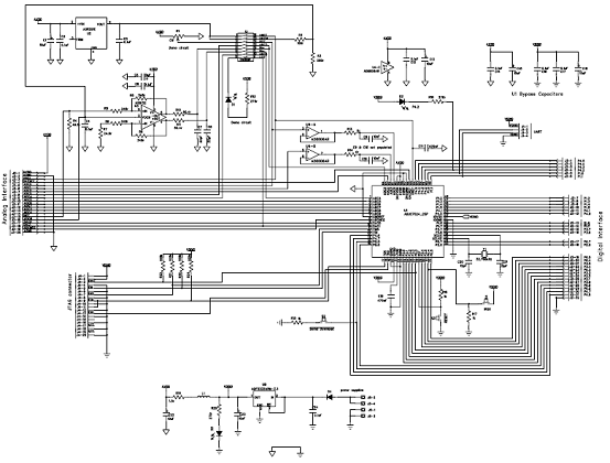
图3.ADuC7024评估板电路图 ADuC7024评估板材料清单: 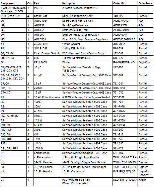
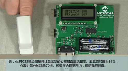
ADI脉搏血氧仪解决方案 脉搏血氧仪以非介入方式测量血液中的含氧量,它以完全饱和水平的百分比来衡量,用单一数值来表示,即所谓血氧饱和百分比,常常称之为SpO2。该测量基于血液中血红蛋白的光吸收特性。在可见光谱和近红外光谱内,含氧血红蛋白(HbO2)与脱氧血红蛋白(Hb)具有不同的吸收曲线。Hb吸收的红光频率的光线较多,红外光(IR)频率的光线较少。HbO2则相反,吸收的红光频率的光线较少,红外光(IR)频率的光线较多。红光和红外光LED尽可能相互靠近,通过人体中的单一组织位置透射光线。红光和红外光LED采用时间复用处理来透射光线,因此不会相互干扰。环境光线经过估算后,从红光和红外光信号中减去。一个能够响应红光和红外光的光电二极管接收光线,然后由一个跨导放大器产生与所接收光线强度成比例的电压。光电二极管接收的红光与红外光的比值用于计算血液中的氧气百分比。根据血液流动的脉冲特性,还会在测量周期中确定并显示脉搏率和强度。 脉搏血氧仪包括发射路径、接收路径、显示和背光、数据接口以及音频报警。发射路径包括红光LED、红外光LED和用于驱动LED的DAC。接收路径包括光电二极管传感器、信号调理、模数转换器和处理器。 脉搏血氧仪系统设计考虑和主要挑战 设计脉搏血氧仪系统时,需要解决多个难题,如低血流灌注、运动和皮肤湿度、杂散光干扰、碳氧血红蛋白和高铁血红蛋白干扰等。 • 低血流灌注(小信号水平)。光电二极管测量需要宽动态范围和低噪声增益的信号调理,以便捕捉脉搏事件。发射和接收路径需要具有高分辨率DAC的高质量、低噪声LED驱动电路和具有高分辨率ADC的高精度模拟前端电路。 • 运动和皮肤湿度。运动会引起伪像,这可以通过软件算法来解决,或者利用ADXL345等加速度计来检测并解决。 • 杂散光干扰。使用光电二极管来响应红光和红外光,它很容易受环境光干扰。因此,用于过滤出红光和红外光目标信号的算法非常重要,这意味着信号处理更加复杂。这种情况下,需要使用具有更高信号处理能力的DSP。 • 碳氧血红蛋白和高铁血红蛋白。一氧化碳(CO)很容易与血红蛋白结合,使血液变得更像红色HbO2,导致测得的SpO2值虚高。血红素基中的铁处于异常状态,无法携带氧(Fe+3而不是Fe+2),导致血红蛋白减少,SpO2读数虚低。使用更多波长可以提高精度,但这需要更高性能的数字处理DSP。处理时间至关重要。 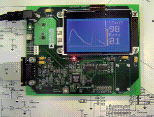
图4. 脉搏血氧仪解决方案外形图 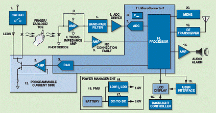
图5.脉搏血氧仪功能框图 脉搏血氧仪功能框图中主要元件表: 
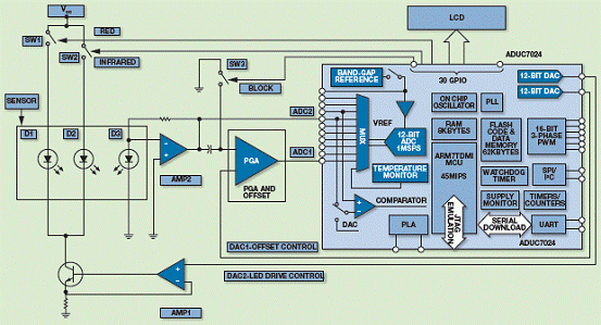
图6. 脉搏血氧仪演示系统框图 脉搏血氧仪应用主要产品表: 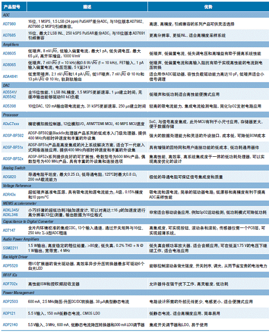
详情请见:  ADuC7019_20_21_22_24_25_26_27_28_29[2].pdf
(1.27 MB)
 69637969AN_719_0[2].pdf
(360.45 KB)
 SPO2_solution_cn[2].pdf
(1.93 MB)
|


网友评论