ADI ADL5304高速200dB对数转换解决方案
发布时间:2011-10-21 14:46
发布者:1046235000
|
ADI 公司的确ADL5304是高速200dB测量范围的对数转换器,具有快速响应和低噪音,正常对数斜率10 mV/dB(200 mV/decade),单电源工作的输入电流在1pA到3mA,双电源工作的输入电流可扩展至10mA,输入电流大于1uA时的带宽大于4MHz,主要用在高精度光功率测量,宽范围基带对数压缩和高速APC回路的检测.本文介绍了ADL5304主要特性,简化方框图,多种参数测量电路图以及单电源工作基本连接图,评估板电路图和PCB布局图. The ADL5304 is a high speed logarithmic converter with fast response and low noise over a 200 dB (1 pA to 10 mA) measurement range. The ADL5304 provides a nominal logarithmic slope of 10 mV/dB (200 mV/decade); other values are easily configured. Logarithmic intercept can be programmed over a wide range with the internal 100 nA current source or externally for log ratio applications. The default intercept value of 3.162 fA places the midpoint of the measurement range of 100 nA at VLOG = 1.5 V. A single positive supply of 5 V is all that is required for operation over a specified 1 pA to 3 mA input range. Dual-supply operation extends the specified input current range to 10 mA. The ADL5304 accepts two current inputs to the logarithmic argument. The numerator input, INUM, flows in the collector of an NPN transistor, connected in a feedback path around a low offset JFET amplifier. The denominator current, IDEN, is treated in the same way, which allows for log ratio operation. The input summing nodes (INUM and IDEN) operate at a constant default voltage of 1.5 V. The VSM1 to VSM4 pins flank the INUM and IDEN inputs to provide a guard voltage to minimize leakage currents. Adaptive photodiode biasing is provided for optical measurements. A monitor current 1.1 times INUM is output at the IMON pin, and an external resistor, RMNTR, at 10 times the photodiode series resistance (RS) applies a voltage across the photodiode that 1st order keeps the internal PD junction at 0 V to minimize dark current. The VLOG output is buffered and can be rescaled through internal gain setting resistors. The internal ILOG varies from −400 μA to +400 μA as INUM changes over 10 decades from 1 pA to 10 mA. This corresponds to 0.5 V to 2.5 V at the VLOG pin in the default configuration shown in Figure 1. Accurate 1.5 V (Pin 1P5V) and 2.0 V (Pin 2VLT) reference outputs allow precise repositioning of the intercept using external resistors. The ADL5304 is available in a 32-lead, 5 mm × 5 mm LFCSP and specified for operation from −40°C to +85°C. ADL5304主要特性: Optimized for very fast response at all input currents Overall bandwidth of >4 MHz for inputs >1 μA Bandwidth: 25 kHz at input of 1 nA and 350 kHz at 10 nA 10 decades of input range: 1 pA to 10 mA Law conformance: ±0.25 dB from 100 pA to 100 μA Log ratio or fixed-intercept operation Precision voltage references and reference current Adaptive photodiode (PD) bias for low dark current Programmable log slope and intercept Default log slope of 10 mV/dB at VLOG pin Single- or dual-supply operation ADL5304应用: High accuracy optical power measurement Wide range baseband log compression Versatile detector for high speed APC loops 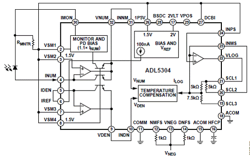
图1.ADL5304简化方框图 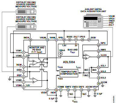
图2.ADL5304测量对数/斜率/失调一致性电路图 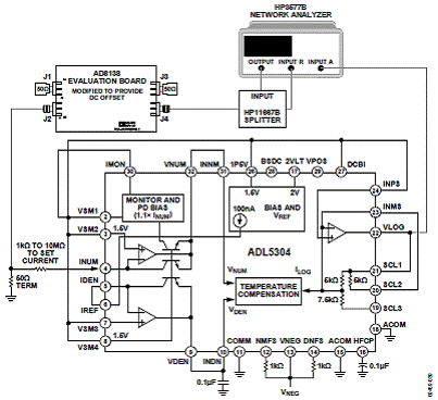
图3.ADL5304测量带宽电路图 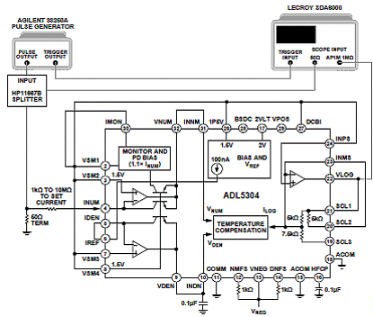
图4.ADL5304测量脉冲设定电路图 
图5.ADL5304测量光电二极管脉冲响应电路图 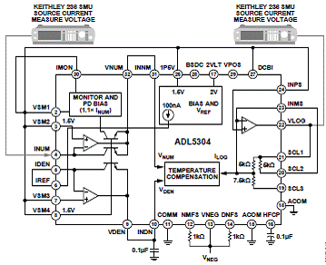
图6.ADL5304测量输出电路图 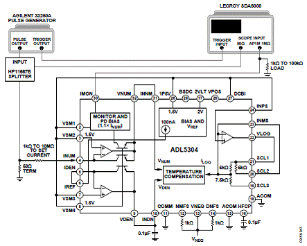
图7.ADL5304测量IMON脉冲响应电路图 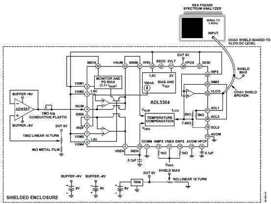
图8.ADL5304测量噪音定电路图: INUM = 100 pA, INUM = 1 nA,和INUM = 10 nA 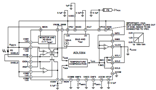
图9.ADL5304单电源工作基本连接图 
图10.ADL5304评估板电路图 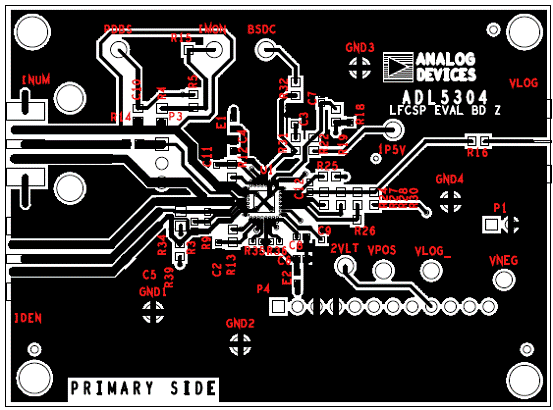
图11.ADL5304评估板PCB布局图 详情请见:  ADL5304[2].pdf
(928.25 KB)
|


网友评论