
ADI ADuC706x基于USB带冷结补偿的热电偶温度监控方案
发布时间:2011-10-13 14:44
发布者:1046235000
|
ADI公司的ADuC7060/ADuC7061均为完全集成的8 kSPS、24位数据采集系统,在单芯片上集成高性能多通道Σ-Δ型模数转换器(ADC)、16位/32位ARM7TDMI® MCU和Flash/EE存储器。器件的电源电压为2.375 V至2.625 V,工作温度范围为−40°C至+125°C工业温度范围.主要用在工业自动化和过程控制,智能精密检测系统和4 mA至20 mA环路智能传感器.本文介绍了ADuC7060/ADuC7061主要特性, 功能方框图, 模拟方框图以及单/双电源连接图, 桥接口, RTD接口和热电偶接口电路图.同时还介绍了基于USB且带冷结补偿的热电偶温度监控器主要特性与电路图,评估板电路图和材料清单. ADuC7060/ADuC7061均为完全集成的8 kSPS、24位数据采集系统,在单芯片上集成高性能多通道Σ-Δ型模数转换器(ADC)、16位/32位ARM7TDMI® MCU和Flash/EE存储器。ADC包括一个5通道主ADC和一个最多8通道辅助ADC,可在单端或差分输入模式下工作。片上提供一个单通道缓冲电压输出DAC,通过编程可将DAC输出范围设置为两种电压范围之一。 这些器件通过一个片内振荡器和锁相环(PLL)产生最高达10.24 MHz的内部高频时钟信号。微控制器内核为ARM7TDMI,它是一个16位/32位RISC机器,峰值性能最高可达10 MIPS。片内集成有4 KB SRAM和32 KB非易失性Flash/EE存储器。ARM7TDMI内核将所有存储器和寄存器视为一个线性阵列。 ADuC7060/ADuC7061包含4个定时器。定时器1是唤醒定时器,能将器件从省电模式唤醒;定时器2可以配置为看门狗定时器。另外还提供一个具有6个输出通道的16位PWM。ADuC7060/ADuC7061内置一个高级中断控制器。该矢量中断控制器(VIC)可以为每个中断分配一个优先级。它还支持嵌套中断,每个IRQ和FIQ最多允许8级嵌套。如果将IRQ和FIQ中断源合并,则可以支持总计16级嵌套中断。片内出厂固件支持通过UART串行接口端口进行在线连续下载,并且支持通过JTAG接口进行非介入仿真。 这些器件的电源电压为2.375 V至2.625 V,工作温度范围为−40℃至+125℃工业温度范围。 The ADuC706x series are fully integrated, 8 kSPS, 24-bit data acqui-sition systems incorporating high performance multichannel sigma-delta (Σ-Δ) analog-to-digital converters (ADCs), 16-bit/ 32-bit ARM7TDMI® MCU, and Flash/EE memory on a single chip. The ADCs consist of a primary ADC with two differential pairs or four single-ended channels and an auxiliary ADC with up to seven channels. The ADCs operate in single-ended or differential input mode. A single-channel buffered voltage output DAC is available on chip. The DAC output range is programmable to one of four voltage ranges. The devices operate from an on-chip oscillator and a PLL gene-rating an internal high frequency clock up to 10.24 MHz. The microcontroller core is an ARM7TDMI, 16-bit/32-bit RISC machine offering up to 10 MIPS peak performance; 4 kB of SRAM and 32 kB of nonvolatile Flash/EE memory are provided on chip. The ARM7TDMI core views all memory and registers as a single linear array. The ADuC706x contains four timers. Timer1 is a wake-up timer with the ability to bring the part out of power saving mode. Timer2 is configurable as a watchdog timer. A 16-bit PWM with six output channels is also provided. The ADuC706x contains an advanced interrupt controller. The vectored interrupt controller (VIC) allows every interrupt to be assigned a priority level. It also supports nested interrupts to a maximum level of eight per IRQ and FIQ. When IRQ and FIQ interrupt sources are combined, a total of 16 nested interrupt levels is supported. On-chip factory firmware supports in-circuit serial download via the UART serial interface ports and nonintrusive emulation via the JTAG interface. The parts operate from 2.375 V to 2.625 V over an industrial temperature range of −40°C to +125°C. ADuC7060/ADuC7061主要特性: Analog input/output Dual (24-bit) ADCs Single-ended and differential inputs Programmable ADC output rate (4 Hz to 8 kHz) Programmable digital filters Built-in system calibration Low power operation mode Primary (24-bit) ADC channel 2 differential pairs or 4 single-ended channels PGA (1 to 512) input stage Selectable input range: ±2.34 mV to ±1.2 V 30 nV rms noise Auxiliary (24-bit) ADC: 4 differential pairs or 7 single-ended channels On-chip precision reference (±10 ppm/°C) Programmable sensor excitation current sources 200 μA to 2 mA current source range Single 14-bit voltage output DAC Microcontroller ARM7TDMI core, 16-/32-bit RISC architecture JTAG port supports code download and debug Multiple clocking options Memory 32 kB (16 kB × 16) Flash/EE memory, including 2 kB kernel 4 kB (1 kB × 32) SRAM Tools In-circuit download, JTAG based debug Low cost, QuickStart™ development system Communications interfaces SPI interface (5 Mbps) 4-byte receive and transmit FIFOs UART serial I/O and I2C (master/slave) On-chip peripherals 4× general-purpose (capture) timers including Wake-up timer Watchdog timer Vectored interrupt controller for FIQ and IRQ 8 priority levels for each interrupt type Interrupt on edge or level external pin inputs 16-bit, 6-channel PWM General-purpose inputs/outputs Up to 14 GPIO pins that are fully 3.3 V compliant Power AVDD/DVDD specified for 2.5 V (±5%) Active mode: 2.74 mA (@ 640 kHz, ADC0 active) 10 mA (@ 10.24 MHz, both ADCs active) Packages and temperature range Fully specified for −40℃ to +125℃ operation 32-lead LFCSP (5 mm × 5 mm) 48-lead LFCSP and LQFP Derivatives 32-lead LFCSP (ADuC7061) 48-lead LQFP and 48-lead LFCSP (ADuC7060) ADuC7060/ADuC7061应用: 工业自动化和过程控制 智能精密检测系统,4 mA至20 mA环路智能传感器 
图1.ADuC7060/ADuC7061功能方框图 
图2.ADuC706x模拟方框图 
图3.ADuC706x外接双电源连接图 
图4.ADuC706x外接单电源连接图 
图5.ADuC706x桥接口电路图 
图6.ADuC706x RTD接口电路图 
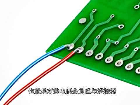
图7.ADuC706x热电偶接口电路图 利用精密模拟微控制器ADuC7060/ADuC7061构建 基于USB且带冷结补偿的热电偶温度监控器 本电路显示如何在精密热电偶温度监控应用中使用精密模拟微控制器ADuC7060/ADuC7061。ADuC7060/ADuC7061集成双通道24位Σ-Δ型ADC、双通道可编程电流源、14位DAC、1.2 V内部基准电压源、ARM7内核、32 kB闪存、4 kB SRAM以及各种数字外设,例如UART、定时器、SPI和I2C接口等。 在本电路中,ADuC7060/ADuC7061连接到一个热电偶和一个100 Ω Pt RTD。RTD用于执行冷结补偿。 在源代码中,ADC采样速率选择100 Hz。当ADC输入PGA的增益配置为32时,ADuC7060/ADuC7061的无噪声分辨率大于18位。 
图8.ADuC7060/ADuC7061用作温度监控控制器与热电偶接口电路 
图9.本电路所用的EVAL-ADUC7061MKZ板外形图 
图10. EVAL-ADUC7061MKZ板电路图(1) 
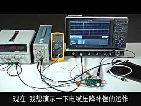
图11. EVAL-ADUC7061MKZ板电路图(2) EVAL-ADUC7061MKZ板材料清单见: 详情请见:  ADuC7060_7061.pdf
(929.19 KB)
CN0214.pdf
(405 KB)
ADuC7060_7061.pdf
(929.19 KB)
CN0214.pdf
(405 KB)
|


网友评论