
NXP TDF8554J I2C总线控制4x45W音频功率放大方案
发布时间:2011-9-24 22:55
发布者:1046235000
|
NXP公司的TDF8554J 是集成了多个电压稳压器和两个功率开关的I2C总线控制的4x45W音频功率放大器.放大器采用基于SOI的BCD工艺,采用互补的DMOS输出级,具有大输出信号和完美的声音质量.器件工作电压可低至6V,I2C总线模式(3.3V和5V兼容),能驱动2欧姆或4欧姆负载,扬声器故障检测,可编程增益 (26 dB和16 dB),主要用在汽车音频系统.本文介绍了TDF8554J 主要特性和优势,方框图, 地线损耗和VP损耗测量电路图,以及测量和应用电路图与PCB元件布局图. The TDF8554J is one of a new generation of complementary quad Bridge-Tied Load (BTL) audio power amplifiers with full I2C-bus controlled diagnostics, multiple voltage regulator and two power switches intended for automotive applications. The TDF8554J can operate at a battery voltage as low as 6 V making this amplifier suitable for stop/start-car operation. The amplifier uses a complementary DMOS output stage in a Silicon-On-Insulator (SOI)-based BCD process. The DMOS output stage ensures a high power output signal with perfect sound quality. The SOI-based BCD process ensures a robust amplifier, where latch-up cannot occur, with good separation between the four independent channels with every component isolated and without substrate currents. The multiple voltage regulator comprises four programmable voltage regulators, one standby regulator and two power switches. The TDF8554J is soft- and hardware downwards-compatible with its predecessor TDA8589XJ. The TDF8554J includes features, such as selectable undervoltage for stop/start-cars which can be selected with additional I2C-bus instruction bytes. If these additional bytes are not sent, the TDF8554J has the same functionality as its predecessor IPAS TDA8589XJ. TDF8554J 主要特性和优势: Amplifier Stop/start-car prepared: keeps operating without audible disturbance during engine start at a battery voltage as low as 6 V I2C-bus mode (3.3 V and 5 V compliant) Can drive 2 ohm or 4ohm loads Speaker fault detection Start-up diagnostics with load detection: open, short, present; filtered for door-slam and chatter relays AC load (tweeter) detection with low and high current mode Gain select after start-up without audible disturbance Programmable gain (26 dB and 16 dB), independently programmable for the front and rear channels Line driver mode (16 dB and mid-tap voltage 0.25VP for stop/start-cars) Programmable clip detection: 2 %, 5 % or 10 % Programmable thermal pre-warning If the temperature protection of the regulator is activated, the amplifier is muted before the regulator is switched off Loss of ground and open VP safe (with 150 m series impedance and a maximum supply decoupling capacitor of 2200 F) All amplifier outputs short-circuit proof to ground, supply voltage and across the load (channel independent) All pins short-circuit proof to ground Temperature-controlled gain reduction to prevent audio holes at high junction Temperatures Programmable low battery voltage detection to enable 7.5 V or 6 V minimum battery voltage operation Overvoltage protection (load-dump safe up to VP = 50 V) and overvoltage pre-warning at 16 V Offset detection Multiple regulator Good stability for any regulator with almost any output capacitor Five voltage regulators (microcontroller, display, audio processor, mechanical digital and mechanical drive) I2C-bus controlled Selectable output voltages for regulators 1, 4 and 5 Low dropout voltage PNP output stages High supply voltage ripple rejection Low noise for all regulators Two power switches (antenna switch and amplifier switch) Standby regulator (microcontroller supply) operational during load dump and thermal shut-down Low standby quiescent current (only regulator 2 operational) Backup functionality for regulator 2 Protection If connection to the battery voltage is reversed, all regulator voltages will be zero Able to withstand output voltages up to 18 V if supply line is short-circuited Thermal protection to avoid thermal breakdown Load-dump protection Regulator outputs protected from DC short-circuit to ground or to supply voltage All regulators protected by foldback current limiting Power switches protected from loss-of-ground 
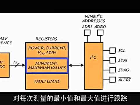
图1. TDF8554J方框图 
图2. TDF8554J地线损耗测量电路图 
图2. TDF8554J VP损耗测量电路图 
图4. TDF8554J测量和应用电路图 
图5. TDF8554J PCB元件布局图(顶层) 详情请见:  TDF8554J[1].pdf
(597.14 KB)
TDF8554J[1].pdf
(597.14 KB)
|
网友评论