TI DAC856x双路16位低功耗电压输出DAC解决方案~*
发布时间:2011-9-2 17:46
发布者:1770309616
|
TI公司的DAC856x, DAC816x和DAC756x系列分别是低功耗电压输出双路16位,14位和12位数模转换器(DAC),集成了2.5-V,4-ppm/°C基准电压,满刻度输出电压范围2.5V或5V,主要用于手提仪表,双极输出,PLC模拟输出模块,闭环伺服控制,压控振荡器, 数据采集系统和可编增益和失调调整.本文介绍了DAC856x主要特性, 方框图, 应用电路以及DAC7562EVM评估板主要特性,电路图和材料清单. The DAC856x, DAC816x, and DAC756x are low-power, voltage-output, dual-channel, 16-, 14-, and 12-bit digital-to-analog converters (DACs), respectively. These devices include a 2.5-V, 4-ppm/℃ internal reference, giving a full-scale output voltage range of 2.5 V or 5 V. The internal reference has an initial accuracy of ±5 mV and can source or sink up to 20 mA at the VREFIN/VREFOUT pin. These devices are monotonic, providing excellent linearity and minimizing undesired code-to-code transient voltages (glitch). They use a versatile three-wire serial interface that operates at clock rates up to 50 MHz. The interface is compatible with standard SPI, QSPI, Microwire, and digital signal processor (DSP) interfaces. DAC856x主要特性: Relative Accuracy: DAC856x (16-Bit): 4 LSB INL DAC816x (14-Bit): 1 LSB INL DAC756x (12-Bit): 0.3 LSB INL Glitch Energy: 0.1 nV-s Bidirectional Reference: Input or 2.5-V Output Output Disabled by Default ±5-mV Initial Accuracy (Max) 4-ppm/℃ Temperature Drift (Typ) 10-ppm/℃ Temperature Drift (Max) 20-mA Sink/Source Capability Power-On Reset to Zero Scale or Mid-Scale Low-Power: 4 mW (Typ, 5-V AVDD, Including Internal Reference Current) Wide Power-Supply Range: 2.7 V to 5.5 V 50-MHz SPI With Schmitt-Triggered Inputs LDAC and CLR Functions Output Buffer With Rail-to-Rail Operation Packages: QFN-10 (3x3 mm), MSOP-10 Temperature Range: –40℃ to 125℃ DAC856x应用: • Portable Instrumentation • Bipolar Outputs (reference design) • PLC Analog Output Module (reference design) • Closed-Loop Servo Control • Voltage Controlled Oscillator • Data Acquisition Systems • Programmable Gain and Offset Adjustment 
图1. DAC856x方框图 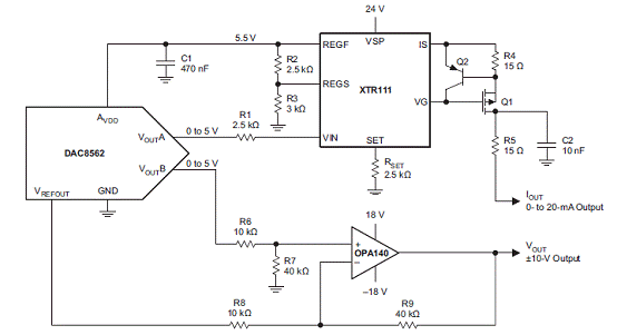
图2. DAC8562 0-20mA/±10-V输出电路图 DAC7562EVM评估板 This user’s guide describes the characteristics, operation, and use of the DAC8562EVM. The evaluation model (EVM) is an evaluation board for the DAC7562 and DAC8562. The DAC7562 and DAC8562 are low-power, voltage-output, 12- or 16-bit digital-to-analog converters (DACs). These converters are controlled through a serial peripheral interface (SPI) that can operate at clock rates of up to 50MHz. Additionally, these DACs include a 2.5V internal reference voltage (disabled by default), giving a full-scale output range of 5V when placed in a gain of two configuration. The EVM allows evaluation of all aspects of the device and allows user control over every pin on the DAC7562/DAC8562. Complete circuit descriptions, schematic diagrams, and bills of material are included in this document. 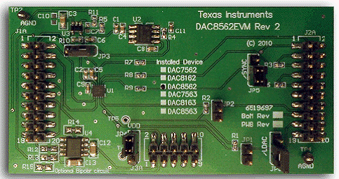
图3. DAC7562EVM评估板外形图 DAC7562EVM评估板主要特性: • Full-featured evaluation board for the DAC7562 or DAC8562 • Onboard optional external reference selection • Wide selection of digital and I/O voltages • Hardware or software control of control logic • Compatible with the TI Modular EVM System • Onboard optional bipolar circuit configuration (requires installing components) 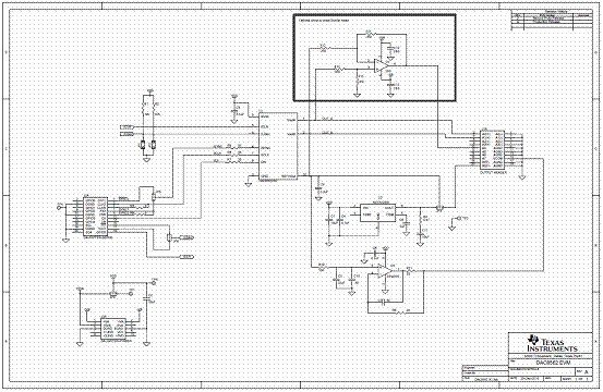
图4.DAC7562EVM评估板电路图 DAC7562EVM评估板材料清单: 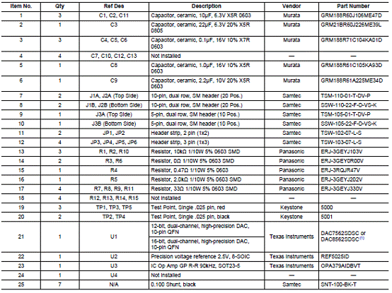
详情请见: http://www.ti.com/lit/ds/symlink/dac8562.pdf 和 http://www.ti.com/lit/ug/sbau183a/sbau183a.pdf |







网友评论