Renesas V850ES-Jx3 移动心电图(ECG)解决方案
发布时间:2011-8-15 12:45
发布者:Liming
|
Renesas 公司的V850ES-Jx3 系列32位MCU包括V850ES/JC3-L系列和V850ES/JE3-L系列,集成了V850ES CPU内核和外设功能如ROM/RAM,定时器/计数器,串行接口,ADC,DAC,主要用在数码相机,电表,移动终端,数字家用电器和其它消费类电子.本文介绍了V850ES-Jx3 系列主要特性,方框图,以及移动心电图(ECG)系统框图和移动心电图(ECG)推荐的元件. The V850ES/Jx3 microcontrollers are equipped with a high-capacity memory of 1 MB. Naturally furnished with functional interchangeability and pin interchangeability with the V850ES/Jx2 microcontrollers and capable of appropriating their development environment as well, the V850ES/Jx3 devices are capable of realizing system acceleration with ease. The newest arrival to the lineup is the V850ES/Jx3-L microcontroller, an ultra-low power-consuming version of the V850ES/JG2 microcontroller, with less than half of its power comsumption current. The V850ES/Jx3-L lineup has achieved an industry-leading nominal power/performance ratio (0.9 mW/MIPS, which comes in under the 1 mW marker according to the Dhrystone evaluation) and actual operating current of 13 mA typ. (at 20 MHz) .Moreover, microcontrollers built in USB (peripheral) function are added in this low power V850ES/Jx3-L product lineup. The V850ES/JC3-L and V850ES/JE3-L are 32-bit single-chip microcontrollers that include the V850ES CPU core and peripheral functions such as ROM/RAM, timer/counters, serial interfaces, an A/D converter, a D/A converter. In addition to high real-time response characteristics and 1-clock-pitch basic instructions, the V850ES/JC3-L and V850ES/JE3-L feature multiply instructions, saturated operation instructions, bit manipulation instructions, etc., realized by a hardware multiplier, as optimum instructions for digital servo control applications. Moreover, as a real-time control system, the V850ES/JC3-L and V850ES/JE3-L enable an extremely high cost-performance for applications that require super low power consumption, such as PC peripheral device, ECR peripheral device, and industrial instrument. V850ES-Jx3 系列主要特性: Minimum instruction execution time: 50 ns (operating on main clock (fXX) of 20 MHz: VDD = 2.7 to 3.6 V) 200 ns (operating on main clock (fXX) of 5 MHz: VDD = 2.2 to 3.6 V) 30.5 s (operating on subclock (fXT) of 32.768 kHz) General-purpose registers: 32 bits 32 registers CPU features: Signed multiplication (16 16 →32): 1 to 2 clocks Signed multiplication (32 32 →64): 1 to 5 clocks Saturated operations (overflow and underflow detection functions included) Most instructions can be executed in 1 clock cycle by using 32-bit RISC-based 5-stage pipeline architecture Instruction fetching from internal ROM and accessing internal RAM for data can be executed separately, by using Harvard architecture High code efficiency achieved by using variable length instructions 32-bit shift instruction: 1 clock cycle Bit manipulation instructions Load/store instructions with long/short format Memory space: 64 MB of linear address space (for programs and data) Internal memory: RAM: 8/16 KB Flash memory: 16/32/64/128/256 KB Interrupts and exceptions: 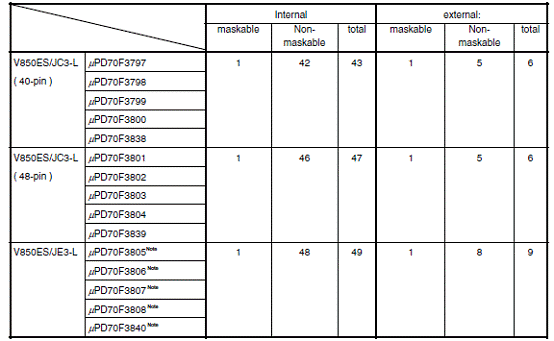
Ports: I/O ports: 27/34/50 Timer function: 16-bit interval timer M (TMM): 1 channel 16-bit timer/event counter P (TMP): 6 channels 16-bit timer/event counter Q (TMQ): 1 channel Watch timer: 1 channel Watchdog timer: 1 channel Real-time counter: 1 channel Real-time output port: 6 bits 1 channel Serial interface: For details about the number of incorporated channels, Asynchronous serial interface A (UARTA) Clocked serial interface B (CSIB) I2C bus interface (I2C) A/D converter: 10-bit resolution: 5/6/10 channels D/A converter: 8-bit resolution: 0/1 channels DMA controller: 4 channels DCU (debug control unit): JTAG interface Clock generator: During main clock or subclock operation 7-level CPU clock (fXX, fXX/2, fXX/4, fXX/8, fXX/16, fXX/32, fXT) Clock-through mode/PLL mode selectable Internal oscillator clock: 220 kHz (TYP.) Power-save functions: HALT/IDLE1/IDLE2/STOP/low-voltage STOP/subclock/sub-IDLE/ low-voltage subclock/low-voltage sub-IDLE mode Package: V850ES/JC3-L 40-pin plastic WQFN (6 6) 48-pin plastic LQFP (fine pitch) (7 7) 48-pin plastic WQFN (7 7) V850ES/JE3-L 64-pin plastic LQFP (fine pitch) (8 8) 64-pin plastic FBGA (5 5) (  D70F3807, 70F3808, 70F3840 only) D70F3807, 70F3808, 70F3840 only) Power supply voltage: VDD = 2.2 V to 3.6 V (5 MHz) VDD = 2.7 V to 3.6 V (20 MHz) Application Fields Digital cameras, electrical power meters, mobile terminals, digital home electronics, other consumer devices V850ES/JC3-L 系列产品列表(1): 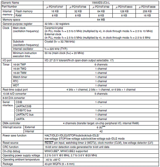
V850ES/JC3-L 系列产品列表(2): 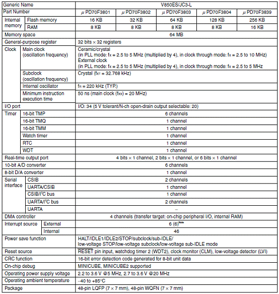
V850ES/JE3-L 系列产品列表(在开发): 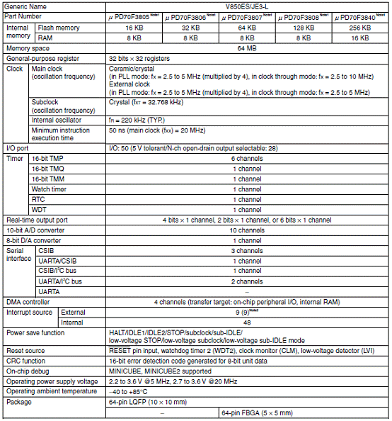
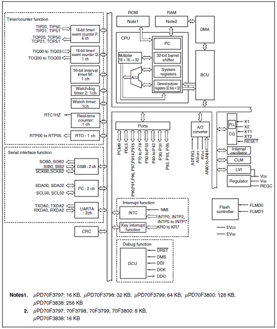
图1.V850ES/JC3-L系列方框图 移动心电图(ECG) A Mobile ECG (Electrocardiograph) is an advance over traditional electrocardiograph units. Its compact size and lightness provide portability, making it possible to measure and record cardiac dysrhythmia anywhere at any time. These small units allow medical personnel to identify cardiac irregularities early on and are very useful for examining patients. Today, though, they are now used not only by healthcare specialists but also by members of the general public. The measurement required to produce an electrocardiogram involves the detection of a variety of electrical potential readings from electrodes taped to the patient’s skin. The electrical potential between a pair of electrodes passes through a highly precise instrumentation amplifier and is read by an A/D converter. A compact electrocardiograph must always be ready to be transported to wherever needed and has to be able to perform reliable data recording. Thus, small size, minimal weight, and extended battery life are essential. The low-power MCUs in the M32C Family and V850ES/Jx3-L from Renesas Electronics are ideal for applications such as compact electrocardiographs. They integrate on-chip an A/D converter for sensor potential detection and provide an LCD drive circuit for the electrocardiogram’s display. This integration helps reduce the overall cost of the system and contributes to the ECG’s compact size, lightness, and long battery life.. 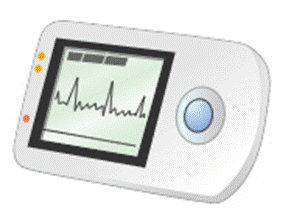
图2.移动心电图(ECG)外形图 
图3.移动心电图(ECG)系统框图 移动心电图(ECG)推荐的元件:
详情请见: http://www2.renesas.com/maps_download/pdf/R01UH0018EJ0100_V850ESJX3L.pdf 和 http://www.renesas.com/media/applications/solutioncatalog/mobile_ecg.pdf |


网友评论