
CMOS集成电路ESD防护设计课程
|
2015年5月6号(周三),我们将在上海主办CMOS集成电路ESD防护设计课程。详细课程请参考附件内容,同时也可以通过点击链接通过网络注册报名。 希望大家能带着问题来,可以当场询问,探讨,交流,多与老师互动,同时我们也会考虑对有ESD需求的客户安排定制的咨询服务,可以安排上门拜访,名额有限,时间另定。 这次ESD防护设计课程主要讲授在先进工艺平台, 高速电路, 无线界面, 特别耐高压等设计方面, 以及在特殊环境应用领域的汽车电子, 工业产品方面的ESD问题探讨和设计。通过这次课程, 让学员更清楚得了解在高密度, 小型化, 复杂功能电子设备设计的背景下, 如何实现减少ESD 设计面积, 设计时间, 提高IC性能和完成苛刻的ESD/ LATCH-UP, EOS等各项指标的要求。随着IC先进制程技术的应用, 芯片功能的增多和尺寸的减小, 对于半导体厂和设计公司来说, 不断面临着产品对静电保护ESD提出的越来越高的要求。 这次授课老师为Bart Keppens,ESD/EOS领域的专业权威人士,丰富的工业界ESD防护设计经历,2002年之前就职于IMEC(比利时微电子研究中心),现任Sofics 公司Director Technical Marketing。SOFICS, 作为欧洲ESD和EOS 领域的资深企业, 早已成为TSMC IP中心, 设计中心的联盟成员, 也是UMC的合作伙伴。ESD IP覆盖一直到了28nm的先进工艺制程,与此同时, 在新的工艺平台SOI, 3D-IC, FINFETs方面, 公司也提出了创新的ESD解决方案。 CMOS集成电路ESD防护设计课程- Advanced ESD Protection Design in CMOS Integrated Circuits Why Participate: The course will provide an overview of the typical issues designers face when they want to protect their circuits against Electrostatic Discharge. Through a set of basic and advanced case studies different on-chip ESD protection concepts are compared. IC designers continue to combine ever more features in advanced digital Systems-on-Chips (SoCs) like analog to digital and digital to analog conversion, sensor interfaces, audio/video handling, high speed interfaces, optical links... The design of these circuits is complex and involves combining IP blocks from different sources. On top of this functional design complexity, circuit designers face challenges related to ESD protection: on-chip ESD concepts used in general purpose I/O’s are not well suited for many specialty interfaces because they introduce high parasitic capacitance, series resistance and leakage current. Similar problems exist in BCD platforms for automotive applications and other high voltage applications. E.g. the amount of electronic circuits in cars has been steadily increasing to an average of more than 50 ASICs per car. Not only the number of circuits in cars has been expanding. Also the quality requirements have been continuously increasing. While on-chip ESD requirements are being lowered in consumer electronics the specifications for automotive parts have only been increased. LIN/CAN interfaces for instance must pass stringent system level ESD stress (IEC 61000-4-2) of more than 6kV. This increased requirement strongly limits the options for ESD protection. Furthermore there are many non-ESD requirements that affect the selection of the most appropriate ESD concept: Electrical OverStress (EOS), Electromagnetic compatibility (EMC) and of course (transient) latch-up. Drastic changes to the process platform (SOI, 3D-IC, FinFETS) can also cause new ESD challenges.
This course has been developed for several categories of designers: * Managers of design teams of ESD/EMC, analog IP blocks and circuits, and their designers. * ESD Specialist/Engineer、 Engineers correlated with Engineering/Quality、System Engineer * Designers with ESD experience, to update their ESD knowledge and to tune their experience to the present-day design procedures.
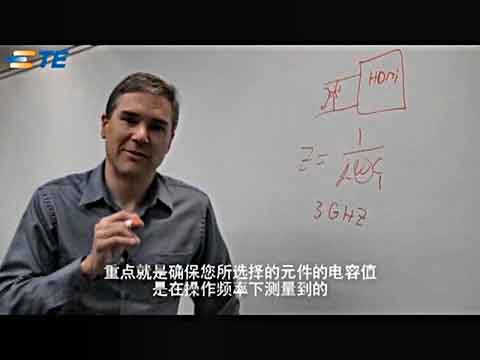
Lynne Consulting is offering advanced engineering courses in the field of analog, RF and mixed-signal IC design targeting the audience of electrical engineers, company managers and marketing engineers working in the semiconductor industry. The lecturers are leading practitioners and top experts in the area from high-technology companies and universities, who teach the most up-to-date information available at the time of the course. Course Details: * Duration: 1 day(6th May 2015) *Location:Building 21, No 1388, Zhangdong Road, Pudong New District, Shanghai, China * Fees:¥1200/person,A discount applies for groups before 22nd April 2015 (2 persons(Total:¥2180);3 persons(Total:¥3100);4 persons or more(negotiation)) * ¥800/person for students * The above discount can not apply simultaneously *Contact us:(Steven.Yu,021-58978665,Email:steven.yu@lynneconsulting.com) The Course Schedule: THEME 1:Introduction - Reason for On-chip ESD protection THEME 2:ESD design window - Concept - ESD test models THEME 3:ESD protection approach overview - Device types - Protection concepts THEME 4:ESD protection for advanced CMOS - Analog interfaces - Advanced CMOS nodes - High voltage tolerant interfaces - Wireless interfaces - High speed interfaces - ESD protection in SOI processes - Sofics approach and track records
- ESD protection in high voltage - Automotive, industrial applications - Sofics approach and track records
- Summary - Trends - Tools - Conclusions Lecturer’s Biography:
From May 2002 he joined Sarnoff Europe, Belgium, solving ESD related problems for customers worldwide, first as ESD engineer, later as technical leader, ESD design specialist. From 2006, Bart supports the Business Development initiatives as Technical Director for ESD. After a management buy-out in June 2009, Sarnoff Europe became 'SOFICS - Solutions for ICs' where Bart is Director Technical Marketing working with semiconductor companies worldwide. Bart (co-) authored more than 25 peer-reviewed published articles in the field of ‘on-chip ESD protection and testing’ and ‘Non Volatile Memories’. Invited papers on ESD solutions and TLP analysis techniques have been delivered at the RCJ ESD symposium in Japan every year between 2006 - 2012. He is member of the Technical Program Committee (‘TPC’) of the EOS/ESD symposium since 2003, member of the ESREF TPC in 2003, 2005, 2007, 2009 and 2010 and member of the Taiwan ESD and Reliability conference TPC since 2010. Bart acted as a Workshop Panelist on ESD topics during various conferences (EOS/ESD Symposium and RCJ) and presented invited tutorials at Taiwan ESD and Reliability conference in 2008, 2010 and 2012. Bart holds several on-chip ESD protection design patents. About Sofics: Sofics is the world leader in on-chip electrostatic discharge (ESD) and electrical overstress (EOS) solutions for ICs. Our technology is proven in all of the world’s major foundries and process nodes, and has been successfully implemented in over a thousand chip designs from IC companies of all sizes. Our TakeCharge portfolio of on-chip solutions offers unique advantages in any IC design requiring custom or specialty I/Os, from 0.18um down to 28nm. TakeCharge technology enables twice the I/O performance in applications that run at high frequencies or high speeds. In low-power applications it delivers ESD protection with leakage that is orders of magnitude lower than generic solutions. When applications call for more robust ESD/EOS protection, TakeCharge outperforms all other approaches while occupying far less silicon area. Sofics also offers PowerQubic technology, a breakthrough in delivering robust on-chip EOS solutions in high-voltage applications. PowerQubic handles all system-level ESD/EOS requirements. We also partner with other IC experts to develop integrated design solutions for specialized applications CustomIO. Sofics recently collaborated with ICsense to build a stable, fully ESD- protected I/O in both 40nm and 28nm that interfaces 1.8V gates with legacy 3.3V off-chip devices. Sofics solutions are highly cost-effective. An IP license from Sofics is more economical than adding staff to an ESD department or hiring a consultant. It is also more cost-efficient than buying shuttle space to develop alternative solutions. Since our solutions are foundry and field-proven, licensees get IP that works the first time. This eliminates the need for expensive re-spins and gets the product to market faster. With our large and growing portfolio of patented IP, in most cases the precise ESD/EOS solution you need will be available off the shelf. Our TakeCharge customers include many of the world’s leading IC makers, and our PowerQubic portfolio has been licensed by a top tier foundry to offer to their customers.
课程信息:
|

网友评论